Thank you for visiting nature.com. You are using a browser version with limited support for CSS. To obtain the best experience, we recommend you use a more up to date browser (or turn off compatibility mode in Internet Explorer). In the meantime, to ensure continued support, we are displaying the site without styles and JavaScript.
- View all journals
- Explore content
- About the journal
- Publish with us
- Sign up for alerts
- Correspondence
- Published: 04 October 2023

The expectations and requirements of research papers in electronics
- Mario Lanza ORCID: orcid.org/0000-0003-4756-8632 1
Nature Electronics volume 6 , page 718 ( 2023 ) Cite this article
1677 Accesses
Metrics details
- Electronic devices
With micro- and nanoelectronic devices and circuits, the most important technical requirements are related to performance metrics (mobility and subthreshold swing for transistors, and switching energy and endurance for memristors), reproducibility (yield, variability, reliability and stability) and fabrication processes (the use of a competitive device structure and size, the use of industry-compatible materials and the feasibility of scaling to the wafer level) 1 , 2 . But expecting authors of a research manuscript to fulfil all the potential requirements is unfair. The reason being that no other article published in any journal has ever accomplished such a thing. Nevertheless, referees can, on occasion, have unrealistic expectations — and demands — for an individual research paper. Here I highlight key technical issues that are often raised during the peer-review process of such papers.
Industry, which relies on silicon complementary metal–oxide–semiconductor (CMOS) technology, typically avoids the use of materials with high diffusivity (silver, gold and iridium) because they could contaminate adjacent devices. However, this point needs to be considered in the right context because the materials allowed in each fabrication step of a microchip are different. In the front-end-of-line (FEOL), the restrictions are much more stringent because the contaminants could arrive at (and short) the transistors; in the back-end-of-line (BEOL), these restrictions could be much more relaxed because the distance to the transistors is higher and anti-diffusion barriers are often employed at the interface between the field oxide and the metallic interconnections. There are, for example, commercial memories that use iridium electrodes in the BEOL 3 , and gold liners are often used at the last metallization layer 4 . Companies also often employ gold electrodes in their prototypes 5 , 6 . Therefore, from a technical point of view, it all depends on where the device is integrated in the microchip.
This is a preview of subscription content, access via your institution
Access options
Access Nature and 54 other Nature Portfolio journals
Get Nature+, our best-value online-access subscription
24,99 € / 30 days
cancel any time
Subscribe to this journal
Receive 12 digital issues and online access to articles
111,21 € per year
only 9,27 € per issue
Buy this article
- Purchase on Springer Link
- Instant access to full article PDF
Prices may be subject to local taxes which are calculated during checkout
International Roadmap for Devices and Systems More Moore (IEEE, 2020); https://irds.ieee.org/editions/2020
International Roadmap for Devices and Systems Beyond CMOS (IEEE, 2020); https://irds.ieee.org/editions/2020
Summerfelt, S. R. et al. Ferroelectric capacitor stack etch cleaning methods. US patent 7,220,600 B2 (2007).
Goodman, P. Gold Bull. 35 , 21–26 (2002).
Article Google Scholar
O’Brien, K. P. et al. In IEEE International Electron Devices Meeting (IEDM) 7.1.1–7.1.4 (IEEE, 2021); https://doi.org/10.1109/IEDM19574.2021.9720651
Lin, Y. et al. In IEEE International Electron Devices Meeting (IEDM) 37.2.1–37.2.4 (IEEE, 2021); https://doi.org/10.1109/IEDM19574.2021.9720668
Goda, A. IEEE Trans. Electron Dev. 67 , 1373–1381 (2020).
Automotive Standard Analog: Robustness and Performance (STMicroelectronics, 2022); https://go.nature.com/3rpWeXs
MS/CMOS Platform (Tower Semiconductor, accessed 28 September 2023); https://go.nature.com/3LAhyk3
Saitoh, M. et al. In IEEE International Electron Devices Meeting (IEDM) 375–378 (IEEE, 2020); https://doi.org/10.1109/IEDM13553.2020.9372106
Download references
Author information
Authors and affiliations.
Materials Science and Engineering Program, Physical Science and Engineering Division, King Abdullah University of Science and Technology (KAUST), Thuwal, Saudi Arabia
Mario Lanza
You can also search for this author in PubMed Google Scholar
Corresponding author
Correspondence to Mario Lanza .
Ethics declarations
Competing interests.
The author declares no competing interests.
Rights and permissions
Reprints and permissions
About this article
Cite this article.
Lanza, M. The expectations and requirements of research papers in electronics. Nat Electron 6 , 718 (2023). https://doi.org/10.1038/s41928-023-01049-0
Download citation
Published : 04 October 2023
Issue Date : October 2023
DOI : https://doi.org/10.1038/s41928-023-01049-0
Share this article
Anyone you share the following link with will be able to read this content:
Sorry, a shareable link is not currently available for this article.
Provided by the Springer Nature SharedIt content-sharing initiative
Quick links
- Explore articles by subject
- Guide to authors
- Editorial policies
Sign up for the Nature Briefing newsletter — what matters in science, free to your inbox daily.

Semiconductor Devices: Theory and Application
James M. Fiore, Mohawk Valley Community College
Copyright Year: 2018
ISBN 13: 9781796543537
Publisher: dissidents
Language: English
Formats Available
Conditions of use.
Learn more about reviews.
Reviewed by Yang Zhao, Assistant Professor, Taylor University on 12/16/21, updated 12/23/21
This book discusses the features and applications of the fundamental semiconductor devices such as diodes, bipolar junction transistors, junction field effect transistors, metal oxide semiconductor field effect transistors, and insulated gate... read more
Comprehensiveness rating: 5 see less
This book discusses the features and applications of the fundamental semiconductor devices such as diodes, bipolar junction transistors, junction field effect transistors, metal oxide semiconductor field effect transistors, and insulated gate bipolar transistors. These are the basic devices that are used in industry and they should be covered in an introductory semiconductor or electronic course.
Content Accuracy rating: 4
The features and applications of the semiconductor devices are descripted accurately by the text, the equations, and the graphics in this book.
Some web links are included in this book for the readers to explore the details of some content. However, these links might be removed any time. For example, the link to the datasheet of 1N4148 is invalid now (as December 2021).
Relevance/Longevity rating: 4
The semiconductor devices that are discussed in this book are the popular ones in industry. They are not likely to be discarded in the near future.
The example semiconductor devices might be discontinued by the manufacturers, as the new models will replace the old ones.
Clarity rating: 5
This book introduces the basic concepts with clear definitions and terminologies. It explains the theory and models with mathematical equations and figures. It demonstrates the applications with example problems and computer simulation results.
Consistency rating: 5
Some variable names are listed in Chapter 1 and they are used through the book. The parameter names, their units, and their typical values are listed under some of the equations. The terminologies in this book are the common ones that are used in other books and in industry.
Modularity rating: 5
Each chapter discusses one dedicated topic, and it is easy for the readers to focus on the content. The length of the chapters are almost the same, and it is easy for the instructors to design a course using this book.
Organization/Structure/Flow rating: 5
This book is well organized. It introduces the semiconductor materials at the beginning. It discusses the features and applications of the specific semiconductor devices next. It talks about the concept of the amplifiers. Then it elaborates the specific amplifier circuits using different semiconductor devices.
Interface rating: 4
It is a good arrangement to show some of the figures, circuits, and plots by the side of the text and equations, and it is convenient for the readers to read the text while observing the graphics.
The curves in the same plot are only differentiated by color. If someone would like to print the book in black and write ink, it is difficult to tell which curve represents which signal.
Grammatical Errors rating: 5
There are no grammatical errors found.
Cultural Relevance rating: 5
The cultural relevance issue is not found, since the book is focused on the semiconductor devices, the circuit theories, and the electrical techniques.
There are review questions or problem sets after each chapter with some answers, which makes this book a good textbook to train the students.
The brief introduction to the history of the semiconductor devices and the inventors makes the book interesting to read. This information could be discussed with the students to engage their learning.
Overall, I would recommend adopting this book in an introductory semiconductor or electronic course.
Table of Contents
Chapter 1: Semiconductor Fundamentals
- 1.0 Chapter Objectives
- 1.1 Introduction
- 1.2 Atomic Structure
- 1.3 Crystals
- 1.4 Doped Materials
Chapter 2: PN Junctions and Diodes
- 2.0 Chapter Objectives
- 2.1 Introduction
- 2.2 The PN Junction
- 2.3 Diode Data Sheet Interpretation
- 2.4 Diode Circuit Models
- 2.5 Other Types of Diodes
Chapter 3: Diode Applications
- 3.0 Chapter Objectives
- 3.1 Introduction
- 3.2 Rectification
- 3.3 Clippers
- 3.4 Clampers
Chapter 4: Bipolar Junction Transistors (BJTs)
- 4.0 Chapter Objectives
- 4.1 Introduction
- 4.2 The Bipolar Junction Transistor
- 4.3 BJT Collector Curves
- 4.4 BJT Data Sheet Interpretation
- 4.5 Ebers-Moll Model
- 4.6 DC Load Lines
- 4.7 BJT Switching and Driver Applications
Chapter 5: BJT Biasing
- 5.0 Chapter Objectives
- 5.1 Introduction
- 5.2 The Need For Biasing
- 5.3 Two-Supply Emitter Bias
- 5.4 Voltage Divider Bias
- 5.5 Feedback Biasing
Chapter 6: Amplifier Concepts
- 6.0 Chapter Objectives
- 6.1 Introduction
- 6.2 Amplifier Model
- 6.3 Compliance and Distortion
- 6.4 Frequency Response and Noise
- 6.5 Miller's Theorem
Chapter 7: BJT Small Signal Amplifiers
- 7.0 Chapter Objectives
- 7.1 Introduction
- 7.2 Simplified AC Model of the BJT
- 7.3 Common Emitter Amplifier
- 7.4 Common Collector Amplifier
- 7.5 Common Base Amplifier
- 7.6 Multi-Stage Amplifiers
Chapter 8: BJT Class A Power Amplifiers
- 8.0 Chapter Objectives
- 8.1 Introduction
- 8.2 Amplifier Classes
- 8.3 Class A Operation and Load Lines
- 8.4 Loudspeakers
- 8.5 Power Transistor Data Sheet Interpretation
- 8.6 Heat Sinks
Chapter 9: BJT Class B Power Amplifiers
- 9.0 Chapter Objectives
- 9.1 Introduction
- 9.2 The Class B Configuration
- 9.3 Extensions and Refinements
Chapter 10: Junction Field Effect Transistors (JFETs)
- 10.0 Chapter Objectives
- 10.1 Introduction
- 10.2 JFET Internals
- 10.3 JFET Data Sheet Interpretation
- 10.4 JFET Biasing
Chapter 11: JFET Small Signal Amplifiers
- 11.0 Chapter Objectives
- 11.1 Introduction
- 11.2 Simplified AC Model of the JFET
- 11.3 Common Source Amplifier
- 11.4 Common Drain Amplifier
- 11.5 Multi-stage and Combination Circuits
- 11.6 Ohmic Region Operation
Chapter 12: Metal Oxide Semiconductor FETs (MOSFETs)
- 12.0 Chapter Objectives
- 12.1 Introduction
- 12.2 The DE-MOSFET
- 12.3 DE-MOSFET Biasing
- 12.4 The E-MOSFET
- 12.5 E-MOSFET Data Sheet Interpretation
- 12.6 E-MOSFET Biasing
Chapter 13: MOSFET Small Signal Amplifiers
- 13.0 Chapter Objectives
- 13.1 Introduction
- 13.2 MOSFET Common Source Amplifiers
- 13.3 MOSFET Common Drain Followers
Chapter 14: Class D Power Amplifiers
- 14.0 Chapter Objectives
- 14.1 Introduction
- 14.2 Class D Basics
- 14.3 Pulse Width Modulation
- 14.4 Output Configurations
Chapter 15: Insulated Gate Bipolar Transistors (IGBTs)
- 15.0 Chapter Objectives
- 15.1 Introduction
- 15.2 IGBT Internals
- 15.3 IGBT Data Sheet Interpretation
- 15.4 IGBT Applications
Ancillary Material
About the book.
The goal of this text, as its name implies, is to allow the reader to become proficient in the analysis and design of circuits utilizing discrete semiconductor devices. It progresses from basic diodes through bipolar and field effect transistors. The text is intended for use in a first or second year course on semiconductors at the Associate or Baccalaureate level. In order to make effective use of this text, students should have already taken coursework in basic DC and AC circuits, and have a solid background in algebra and trigonometry along with exposure to phasors. Calculus is used in certain sections of the text but for the most part it is used for equation derivations and proofs, and is kept to a minimum. For students without a calculus background these sections may be skipped without a loss of continuity.
There is also a lab manual for this textbook.
About the Contributors
James M. Fiore
My name is Jim and I'm the resident dissident, programmer and author. I've been a college professor for many years teaching in the areas of electrical engineering technology, computer programming and the science of sound. I'm also a musician and an endurance athlete. I established dissidents in the late 1980s as a way to offer various software items that I created, figuring that other people might find them useful as well. Some of these have been commercial and some have been freeware. I also write a lot, including published college text books and lab manuals. Recently, the open educational resource movement has gained momentum (no doubt at least partly propelled by the rising costs of college tuition and texts).
Contribute to this Page
digital electronics Recently Published Documents
Total documents.
- Latest Documents
- Most Cited Documents
- Contributed Authors
- Related Sources
- Related Keywords
Impact of Molecular Electrostatics on Field-Coupled Nanocomputing and Quantum-Dot Cellular Automata Circuits
The molecular Field-Coupled Nanocomputing (FCN) is a promising implementation of the Quantum-dot Cellular Automata (QCA) paradigm for future low-power digital electronics. However, most of the literature assumes all the QCA devices as possible molecular FCN devices, ignoring the molecular physics. Indeed, the electrostatic molecular characteristics play a relevant role in the interaction and consequently influence the functioning of the circuits. In this work, by considering three reference molecular species, namely neutral, oxidized, and zwitterionic, we analyze the fundamental devices, aiming to clarify how molecule physics impacts architectural behavior. We thus examine through energy analysis the fundamental cell-to-cell interactions involved in the layouts. Additionally, we simulate a set of circuits using two available simulators: SCERPA and QCADesigner. In fact, ignoring the molecular characteristics and assuming the molecules copying the QCA behavior lead to controversial molecular circuit proposals. This work demonstrates the importance of considering the molecular type during the design process, thus declaring the simulators working scope and facilitating the assessment of molecular FCN as a possible candidate for future digital electronics.
Digital electronics using dielectric elastomer structures as transistors
Prototype of the digital electronics chain for the gabriela detector assembly and first tests, inquiry-based learning used for implementation of bcd adders in the course "digital electronics", design and analysis of cntfet based vlsi interconnects by using pvt variation.
Abstract With the quick progress in the area of digital electronics results in miniaturization of semiconductor Industries. In Deep Sub Micron regime, because of leakage current, power consumption is turn out to be a major issue; hence constant efforts are being made by the researchers for investigating the various ways to minimize this. There are various methods available for the same and out of several available methods use of Carbon Nano-tube technology is a promising way to design low power circuits efficiently. Here new techniques are introduced for the reduction of leakage power. Here in this work, comparison of the main performance parameters of Copper on chip nano-interconnect with CNTFET has been done. We have measured the impact of ION and IOFF current by applying Process variation in CU and CNT- Interconnects with the variation of Tubes at 32nm technology and analysed the performance of the digital circuits with scaling of technology. The different kind of simulation outcomes indicates that by applying 10% of deviation from normal value in different device characteristics parameters such as Length of Gate (LTube) of the Tube, Width (WTube) of the Tube, Threshold Voltage (Vth) of the Tube, Thickness (tot) of Tube and Source & Drain Doping concentration with Cu and CNTFET interconnects for NFET and PFET with the variation of tubes from 1 to 16. All the experimental outcomes are achieved by using HSPICE simulator using SPICE model of CU and CNT at27oC temperature by using 32nm Berkley Predictive Technology module.
El software como apoyo didáctico en la enseñanza de la electrónica digital en la educación superior en México [Software as a didactic support in the teaching of digital electronics in higher education in Mexico]
La educación actual ha sufrido diversas modificaciones, sobre todo con la aparición del COVID-19 en el mundo. Entre las herramientas tecnológicas que apoyan la actividad didáctica, están los softwares educativos; éstos permiten la simulación de prácticas en laboratorios virtuales que complementan el aprendizaje y permiten demostrar principios teóricos. En el presente artículo se llevó a cabo un análisis documental sobre el uso del software en la electrónica digital, se elaboró un temario común de la materia electrónica digital de las licenciaturas que oferta el Tecnológico Nacional de México. Finalmente se llevó a cabo un análisis del uso del software determinado hacia la materia en cuestión y se estableció una relación que indica el nivel de adecuación de este. Current education has undergone various modifications, especially with the appearance of COVID-19 in the world. Among the technological tools that support the didactic activity is simulation software; These allow to carry out virtual laboratory practices that complement the learning and allow demonstrating theoretical principles. In this article, a documentary analysis was carried out on the use of software in digital electronics, a common agenda of digital electronic matter of the degrees offered by the Tecnológico Nacional de México was elaborated. Finally, an analysis of the use of the software determined towards the subject in question was carried out and a relationship was established that indicates the level of adequacy. Learning styles were identified in the group of surveyed students, and their relationship with the level of satisfaction and achievement of the software.
PROJECT-BASED LEARNING APPROACH USED FOR TEACHING AND LEARNING THE TOPIC “BCD ADDERS” IN THE COURSE “DIGITAL ELECTRONICS” DURING COVID-19 PANDEMIC
Active learning for teaching “synthesis and analysis of counters” in the course “digital electronics”, project-based learning approach applied in the course “digital electronics” for studying the topic “binary multipliers”, si-based mems resonant sensor: a review from microfabrication perspective.
With the technological advancement in micro-electro-mechanical systems (MEMS), microfabrication processes along with digital electronics together have opened novel avenues to the development of small-scale smart sensingdevices capable of improved sensitivity with a lower cost of fabrication and relatively small power consumption. This article aims to provide the overview of the recent work carried out on the fabrication methodologies adoptedto develop silicon based resonant sensors. A detailed discussion has been carried out to understand critical steps involved in the fabrication of the silicon-based MEMS resonator. Some challenges starting from the materialsselection to the ?final phase of obtaining a compact MEMS resonator device for its fabrication have also been explored critically.
Export Citation Format
Share document.
3D-printing and advanced manufacturing for electronics
- Review Article
- Published: 04 February 2019
- Volume 4 , pages 245–267, ( 2019 )
Cite this article

- Alejandro H. Espera Jr. ORCID: orcid.org/0000-0002-3294-1847 1 , 2 ,
- John Ryan C. Dizon 1 , 3 ,
- Qiyi Chen 1 &
- Rigoberto C. Advincula 1
6993 Accesses
192 Citations
2 Altmetric
Explore all metrics
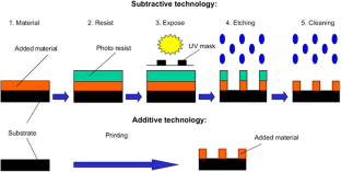
Printed electronics currently holds a significant share in the electronics fabrication market due to advantages in high-throughput production and customizability in terms of material support and system process. The printing of traces and interconnects, passive and active components such as resistors, capacitors, inductors, and application-specific electronic devices, have been a growing focus of research in the area of additive manufacturing. Adaptation of new 3D-printing technologies and manufacturing methods, specifically for printed electronics, are potentially transformative in flexible electronics, wireless communications, efficient batteries, solid-state display technologies, etc. Other than printing new and reactive functional electronic materials, the functionalization of the printing substrates with unusual geometries apart from the conventional planar circuit boards will be a challenge. Building the substrate, printing the conductive tracks, pick-and-placing or embedding the electronic components, and interconnecting them, are fundamental fabrication protocols new 3D-printing systems should adopt for a more integrated fabrication. Moreover, designers and manufacturers of such systems will play an important role in scaling 3D-printed electronics from prototyping to high-throughput mass production. This review gives a groundwork for such understanding, defining methods and protocols, reviewing various 3D-printing methods, and describing the state-of-the-art in 3D-printed electronics and their future growth.
This is a preview of subscription content, log in via an institution to check access.
Access this article
Price includes VAT (Russian Federation)
Instant access to the full article PDF.
Rent this article via DeepDyve
Institutional subscriptions
A Review on Printed Electronics with Digital 3D Printing: Fabrication Techniques, Materials, Challenges and Future Opportunities

3D Printing: Printed Electronics

Recent advances in direct ink writing of electronic components and functional devices
Nature (2018) “Electronic devices”. https://www.nature.com/subjects/electronic-devices . Accessed 24 Oct 2018
Research B (2017) “Global Electronics Components Market Sees Continued Growth (7.7% CAGR),” GlobeNewswire, 9 October 2017. https://globenewswire.com/news-release/2017/10/09/1142799/0/en/Global-Electronics-Components-Market-Sees-Continued-Growth-7-7-CAGR.html . Accessed 24 Oct 2018
Cook B, Tehrani B, Cooper J, Kim S, Tentzeris M (2015) Integrated printing for 2D/3D flexible organic electronic devices. Handbook of flexible organic electronics. Woodhead Publishing, Cambridge, pp 199–216
Google Scholar
Weiderrecht G (2009) Handbook of nanofabrication. Elsevier, New York
Mosses R, Brackenridge S (2003) A novel process for the manufacturing of advanced interconnects. Circuit World 29(3):18–21
Article Google Scholar
Zhao D, Liu T, Lin Z, Zhang M, Liang R, Wang B (2012) Fabrication and characterization of aerosol-jet printed strain sensors for multifunctional composite structures. Smart Mater Struct 21(11):115008
Lu B, Li D, Tian X (2015) Development trends in additive manufacturing and 3D printing. Engineering 1:85–89,
Shirasaki Y, Supran G, Bawendi M, Bulović V (2012) Emergence of colloidal quantum-dot light-emitting technologies. Nat Photonics 7:13–23
Dizon J, Espera A, Chen Q, Advincula R (2017) Mechanical characterization of 3D-printed polymers. Additive Manuf 20:44–67
Macdonald E, Salas R, Espalin D, Perez M, Aguilera E, Muse D, Wicker R (2014) 3D printing for the rapid prototyping of structural electronics. IEEE Access 2:234–242
Macdonald E (2012) Integrating stereolithography and direct print technologies for 3D structural electronics fabrication. Rapid Prototyping J
Ahn B, Duoss E, Motala M, Guo X, Park S-I, Xiong Y, Yoon J, Nuzzo R, Rogers J, Lewis J (2009) Omnidirectional Printing of Flexible, Stretchable, and Spanning Silver Microelectrodes. Science 323(5921):1590–1593
Lewis J, Ahn B (2015) Three-dimensional printed electronics. Nature 518:42–43
NanoMarkets Report (2007) Printed electronics: a manufacturing technology analysis and capability forecast 2007. http://www.nanomarkets.net . Accessed 2 June 2017
All About Circuits (2017) Active vs passive devices. https://www.allaboutcircuits.com/textbook/semiconductors/chpt-1/active-versus-passive-devices/ . Accessed 13 Jun 2017
Poole I (2017) What is SMT surface mount technology—tutorial. http://www.radio-electronics.com/info/data/smt/what-is-surface-mount-technology-tutorial.php . Accessed 25 Jun 2017
NanoMarkets L (2005) NanoMarkets printable electronics report 2005. http://www.nanomarket.net/
Gibson I, Rosen D, Stucker B (2009) Additive manufacturing technologies: 3D printing, rapid prototyping, and direct digital manufacturing. Springer, Berlin
John (2010) ICF techniques, 31 May 2010. http://www.circuitstoday.com/ic-fabrication-techniques . Accessed 2 Jun 2017
Kunnari E, Valkama J, Keskinen M, Mansikkamaki P (2009) Environmental evaluation of new technology: printed electronics case study. J Cleaner Prod 17:791–799
Kipphan H (2011) Handbook of print media. Springer, Germany
Océ D (2006) Printing, 10th ed. Océ Printing Systems GmbH, Poing
Sekitani T, Noguchi Y, Zschieschang U, Klauk H, Someya T (2008) Organic transistors manufactured using inkjet technology with subfemtoliter accuracy. Proc Natl Acad Sci 105(13):4976–4980
Sridhar A, Blaudeck T, Baumann R (2011) Inkjet printing as a key enabling technology for printed electronics. Mater Matters 6(1):12–15
Wood V, Panzer M, Chen J, Bradley M, Halpert J, Bawendi M, Bulovic V (2009) Inkjet-printed quantum dot–polymer composites for full-color AC-driven displays. Adv Mater 21(21):1–5
Derby B (2010) Inkjet printing of functional and structural materials: fluid property requirements, feature stability, and resolution. Annu Rev Mater Res 40:395–414
Professional SPIE (2013) Chuck Hull: pioneer in stereolithography. https://spie.org/membership/spie-professional-magazine/spie-professional-archives-and-special-content/2013-january-spie-professional-archive/chuck-hull . Accessed 11 Jun 2017
Grimm T (2004) User’s guide to rapid prototyping. Society of Manufacturing Engineers, Dearborn
Hull CW (1986) Apparatus for production of three-dimensional objects by stereolithography. US Patent 4,575,330, 11 March 1986
Melchels FPW, Feijen J, Grijpma DW (2010) A review on stereolithography and its applications in biomedical engineering. Biomaterials 31:6121–6130
Waterman N, Dickens P (1994) Rapid product development in the USA, Europe and Japan. World Class Design Manuf 1(3):27–36
Pham D, Gault R (1998) “A comparison of rapid prototyping technologies”. Int J Mach Tools Manuf 38:1257–1287
Campbell T, Williams C, Ivanova O, Garrett B (2011) Could 3D printing change the world? Atlantic Council, Washington
Kazmer D (2001) Three-dimensional printing of plastics. In: Applied plastics engineering handbook—processing, materials, and applications, a volume in plastic design library, Elsevier, New York, pp 617–634
Sachs E, Cima M, Cornie J (1990) Three dimensional printing: rapid tooling and prototypes directly from CAD representation. CIRP Annals Manuf Technol 39(1):201–204
Mota C, Puppi D, Dinucci D, Gazzarri M, CHielleni F (2013) Additive manufacturing of star poly(ε-caprolactone) wetspun scaffolds for bone tissue engineering applications. J Bioact Compatib Polym 28(4):320–340
Lewis J (2006) Direct ink writing of 3D functional materials. Adv Funct Mater 16:2193–2204
de Leon A, Chen Q, Palaganas N, Palaganas J, Manapat J, Advincula R (2016) High performance polymer nanocomposites for additive manufacturing applications. React Funct Polym 103:141–155
Mortara L, Hughes J, Ramsundar PLF, Probert D (2009) Proposed classification scheme for direct wire technologies. Rapid Prototyping J 15(4):299–309
Hon K, Li L, Hutchings I (2008) Direct writing technology—advances and developments. CIRP Ann Manuf Technol 57(2):601–620
Perez K, Williams C (2013) Combining additive manufacturing and direct wire for integrated electronics—a review. In: 24th International solid freeform fabrication symposium—an additive manufacturing conference, Texas
Hoerber J, Glasschroeder J, Pfeffer M, Schilp J, Zaeh M, Franke J (2014) Approaches for additive manufacturing of 3D electronic applications. Proc CIRP 17:806–811
Robinson CJ, Stucker B, Lopes AJ, Wicker R, Palmer JA (2006) Integration of direct-write (DW) and ultrasonic consolidation (UC) technologies to create advanced structures with embedded electrical circuitry. In: 17th solid freeform fabrication symposium, Texas
Medina F, Lopes A, Inamdar A, Hennessey R, Palmer J, Chavez B, Davis D, Gallegos P, Wicker R (2005) Hybrid manufacturing: integrating direct write and stereolithography. In: Solid freeform fabrication symposium proceedings, Austin, TX
Janaki Ram G, Yang Y, George J, Robinson C, Stucker B (2006) Improving Linear Weld Density in Ultrasonically Consolidated Parts. In: Solid freeform fabrication symposium proceedings, Austin, TX
Masurtschak S, Friel R, Gillner A, Ryll J, Harris R (2014) Laser-machined microchannel effect on microstructure and oxide formation of an ultrasonically processed aluminum alloy. J Eng Mater Technol 137(1):011006
3D Printing Processes. https://3dprintingindustry.com/3d-printing-basics-free-beginners-guide/processes/ . Accessed 16 Jul 2017
Manapat J, Chen Q, Ye P, Advincula R (2017) 3D printing of polymer nanocomposites via stereolithography. Macromol Mater Eng 302:1600553
Dizon J, Chen Q, Valino A, Advincula R (2018) Thermo-mechanical and swelling properties of three-dimensional-printed poly(ethylene glycol) diacrylate/silica nanocomposites. MRS Commun. https://doi.org/10.1557/mrc.2018.188
Gebhardt A (2007) Generative manufacturing processes, rapid prototyping–rapid tooling–rapid manufacturing. Carl Hanser, Munich
Zaeh M, Glasschroeder J, Krol T, Schilp J (2011) Innovative solutions for increasing the quality of components at additive manufacturing. Utz, Munich
Gibbson I, Rosen D, Stucker B (2010) Additive manufacturing technologies, rapid prototyping to direct digital manufacturing. Springer, New York
Lee D, Oh J (2010) Inkjet printing of conductive Ag lines and their electrical and mechanical characterization. Thin Solid Films 518(22):6352–6356
Hedges M (2010) 3D aerosol jet printing—an emerging mid manufacturing. In: 9th International congress molded interconnect devices, Fuerth
Teschler L (2015) Your next circuit design could be fabricated on a printer. http://www.powerelectronictips.com/your-next-circuit-design-could-be-fabricated-on-a-printer/ . Accessed 22 Jun 2017
Krebs T (2010) Flexible circuits or printed circuit boards? Technology selection based on virtual prototypes. In: 9th International congress molded interconnect devices, Fuerth
Frank J, Feldmann K, Fischer C (2009) Two approaches for the design of modeled interconnect devices (3D-MID). In: Proceedings 6th international conference on digital enterprise technology, Hongkong
Falat T, Platek B, Felba J (2012) Sintering process of silver nanoparticles in ink-jet printed conductive microstructures—molecular dynamics approach. In: 13th International conference on thermal, mechanical and multi-physics simulation and experiments in microelectronics and microsystems
Allen M (2011) Nanoparticle sintering methods and applications for printed electronics. In: Aalto University publication series, Helsinki
Frank J (2013) Molded interconnect devices 3D-MID: materials, manufacturing, assembly and applications for molded circuit carriers. Carl Hanser, Munich
Pfeffer M, Goth C, Craiovan D, Frank J (2011) 3D-Assembly of molded interconnect devices with standard smd pick & place machines using an active multi axis workpiece carrier. In: International symposium on assembly and manufacturing, IEEE, Tampere
Miettinen J, Pekkanen V, Kaija K, Mansikkamaki P, Mantysalo J, Mantysalo M (2008) Inkjet printed system-in-package design and manufacturing. Microelectron J 39(12):1740–1750
editor OEA (2011) A roadmap for organic and printed electronics. Whitepaper-OE, Frankfurt
Tseng H, Subramanian V (2011) All inkjet-printed, fully self-aligned transistors for low-cost circuit applications. Org Electron 12(2):249–256
Kim D, Lee S, Jeong S, Moon J (2009) All-ink-jet printed flexible organic thin-film transistors on plastic substrates. Electrochem Solid State Lett 12:H195-H197
Saengchairat N, Tran T, Chua C (2017) A review: additive manufacturing for active electronic components. Virtual Phys Prototyp 12:31–46
Tan H, Tran T, Chua C (2016) A review of printed passive electronic components through fully additive manufacturing methods. Virtual Phys Prototyp 11:271–288
Ready S, Arias A, Sambandan S (2009) Ink jet printing devices and circuits. In: Materials research society fall meeting, Boston, MA
Ready S, Wong W, Arias A, Apte R, CHabynic M, Street R, Salleo A (2006) Toolset for printed electronics. In: International conference on digital fabrication technologies, Denver, CO
Ng T, Schwartz E, Lavery L, Whiting G, Krusor RB,B, Veres J, Broms P, Herlogsson L, Alam N, Hagel O, Nilsson J, Karlsson C (2012) Scalable printed electronics: a printed decoder addressing ferroelectric nonvolatile memory. Sci Rep 2:585
Ready S, Endicott F, Whiting G, Ng T, Chow E, Lu J (2013) 3D printed electronics. In: NIP 29 and Digital Fabrication pp 9–12
MacDonald E, Wicker R (2016) Multiprocess 3D printing for increasing component functionality. Science 353:aaf2093
Jung S, Sou A, Gili E, Sirringhaus H (2013) Inkjet-printed resistors with a wide resistance range for printed read-only memory applications. Org Electron 14:699–702
3D-printing basic electronic components (2015) http://www.kurzweilai.net/3d-printing-basic-electronic-components . Accessed 6 July 2017
Wu S-Y, Yang C, Hsu W, Lin L (2015) 3D-printed microelectronics for integrated circuitry and passive wireless sensors. Microsyst Nanoeng 1:15013
Kong Y, Tamargo I, Kim H, Johnson B, Gupta M, Koh T-W, Chin H-A, Steingart D, Rand B, McAlpine M (2014) 3D printed quantum dot light-emitting diodes. Nano Lett 14:7017–7020
Goh G, Ma J, Chua K, Shweta A, Yeong W, Zhang Y (2016) Inkjet-printed patch antenna emitter for wireless communication application. Virtual Phys Prototyp 11:289–294
Adams J, Bernhard J (2009) Tuning method for a new electrically small antenna with low Q. IEEE Antennas Wireless Propag Lett 8:303–306
Adams J, Duoss EB, Malkowski T, Motala M, Ahn B, Nuzzo R, Bernhard J, Lewis J (2011) Conformal printing of electrically snall antennas on three-dimensional surfaces. Adv Mater 23:1335–1340
Baca A, Yu K, Xiao J, Wang S, Yoon J, Ryu J, Stevenson D, Nuzzo R, Rockett A, Huang Y, Rogers J (2010) Compact monocrystalline silicon solar modules with high voltage outputs and mechanically flexible designs. Energy Environ Sci 3:208–211
Rogers J, Bao Z, Baldwin K, Dodabalapur A, Crone B, Raju V, Kuck V, Katz H, Amundson K, Ewing J, Drzaic P (2001) Paper-like electronic displays: large-area rubber-stamped plastic sheets of electronics and microencapsulated electrophoretic inks. Proc Natl Acad Sci/ USA 98(9):4835–4840
Fichet G, Corcoran N, Ho P, Arias A, MacKenzie J, Huck W, Friend R (2004) Self-organized photonic structures in polymer light-emitting diodes. Adv Mater 16:1908
Someya T, Kato Y, Sekitani S, Iba Y, Noguchi Y, Murase H, Kawaguchi, Sakurai T (2005) Conformable, flexible, large-area networks of pressure and thermal sensors with organic transistor active matrixes. Proc Natl Acad Sci USA 102(35):12321–12325
Cao Q, Hur S-H, Zhu Z-T, Sun Y, Wang C, Meitl M, Shim M, Rogers J (2006) Highly bendable, transparent thin-film transistors that use carbon-nanotube-based conductors and semiconductors with elastomeric dielectrics. Adv Mater 18:304–309
Gaikwad A, Whiting G, Steingart D, Arias A (2011) Highly flexible printed alkaline batteries based on mesh embedded electrodes. Adv Mater 23:3251
Liu H, Huang W, Gao J, Dai K, Zheng G, Liu C (2016) Piezoresistive behavior of porous carbon nanotube-thermoplastic polyurethane conductive nanocomposites with ultrahigh compressibility. Appl Phys Lett 108(1):11904
Yao H, Ge J, Wang C, Wang X, Hu W, Zheng Z, Ni Y, Yu S (2013) A flexible and highly pressure-sensitive graphene–polyurethane sponge based on fractured microstructure design. Adv Mater 25(46):6692–6698
Chen Q, Cao P, Advincula R (2018) Mechanically robust, ultraelastic hierarchical foam with tunable properties via 3D printing. Adv Func Mater 28:1800631
Fan YJ, Meng XS, Li HY, Kuang SY, Zhang L, Wu Y, Wang ZL, Zhu G (2017) Stretchable porous carbon nanotube-elastomer hybrid nanocomposite for harvesting mechanical energy. Adv Mater 29(2):1603115
Liu C, Choi J (2009) An embedded PDMS nanocomposite strain sensor toward biomedical applications. In: Engineering in Medicine and Biology Society, annual international conference of the IEEE, pp 6391–6394
Amjadi M, Pichitpajongkit A, Lee S, Ryu S, Park I (2014) “Highly stretchable and sensitive strain sensor based on silver nanowire-elastomer nanocomposite. ACS Nano 8(5):5154–5163
Chen Q, Mangadlao J, Wallat J, de Leon A, Pokorski J, Advincula R (2017) 3D printing biocompatible polyurethane/poly (lactic acid)/graphene oxide nanocomposites: anisotropic properties. ACS Appl Mater Interfaces 9(4):4015–4023
Bates S, Farrow I, Trask R, RG S (2016) 3D printed elastic honeycombs with graded density for tailorable energy absorption. SPIE smart structures and materials + nondestructive evaluation and health monitoring. International Society for Optics and Photonics, Bellingham, p 979907
Christ J, Aliheidari N, Ameli A, Potschke P (2017) 3D printed highly elastic strain sensors of multiwalled carbon nanotube/thermoplastic polyurethane nanocomposites. Mater Design 131:394–401
Muth J, Vogt D, Trugby R, Menguc Y, Kolesky D, Wood R, Lewis J (2014) Embedded 3D printing of strain sensors within highly stretchable elastomers. Adv Mater 26(36):6307–6312
Choi J-H, Wang H, Oh J, Paik T, Jo P, SUng J, Ye X, Zhao T, Murray DBT,C, Kagan C (2016) Exploiting the colloidal nanocrystal library to construct electronic devices. Science 352(6282):205–208
Wehner M, Truby R, Fitzgerald D, Mosadegh B, Whitesides G, Lewis J, Wood R (2016) An integrated design and fabrication strategy for entirely soft, autonomous robots. Nature 536:451–455
Malone E, Bery M, Lipson H (2008) Freeform fabrication and characterization of Zn-air batteries. Rapid Prototyp J 14(3):128–140
Sun K, Wei T-S, Ahn B, Seo J, DIllon S, Lewis J (2013) 3D printing of interdigitated Li-Ion microbattery architecture. Adv Mater 25:4539–4543
MarketsandMarkets (2016) Printed E market by material (Ink, Substrate), technology (inkjet, screen, gravure, flexographic), device (sensors, displays, batteries, rfid, lighting, photovoltaic) and geography—Global forecast to 2022. http://www.marketsandmarkets.com/Market-Reports/printed-electronics-market-197.html . Accessed 8 Jul 2017
Sridhar A (2010) An inkjet printing-based process chain for conductive structures on printed circuit board materials. Thesis PhD, University of Twente, the Netherlands,
Parashkhov R, Becker E, Riedl T, Johannes H-H, Kowalsky W (2005) All-organic thin-film transistors made of poly(3-butylthiophene) semiconducting and various polymeric insulating layers. In: W. Proc. IEEE, vol. 93, no. 7
Vornbrock ADLF, Sung D, Kang H, Kitsomboonloha R, Subramanian V (2010) Fully gravure and ink-jet printed high speed pBTTT organic thin film transistors. Org Electron 11:2037. https://doi.org/10.1016/j.orgel.2010.09.003
Pekkanen J (2007) Sintering of inkjet printed Ag nanoparticles. Master of Science thesis, Tampere, Finland
Lam Research (2017) Products overview: enabling chipmakers to create the future. http://www.lamresearch.com/products/products-overview . Accessed 13 Jun 2017
Gaynor A, Meisel N, Williams C, Guest J (2014) Multi-material topology optimization of compliant mechanisms created via PlyJet three-dimensional printing. J Manuf Sci Eng 136(6):061015
Gibson I, Rosen D, Stucker B (2010) Additive manufacturing technologies. Springer, Boston
Book Google Scholar
Perelaer J, Schubert U, Jena F (2010) Inkjet printing and alternative sintering of narrow conductive tracks on flexible substrates for plastic electronic applications. Radio frequency identification fundamentals and applications, design methods and solutions. InTech, Rijeka, Croatia, pp 265–286
Lee J-Y, An J, Chua C (2017) Fundamentals and applications of 3D printing for novel materials. Appl Mater Today 7:120–133
Download references
Acknowledgements
We would like to thank the Case Western Reserve University through PETRO Case, Honeywell—Kansas City National Security Campus (KCNSC) and the Department of Science and Technology—Philippine Council for Industry, Energy, and Emerging Technology Research and Development (DOST-PCIEERD) for resources and funding in the area of additive manufacturing.
Author information
Authors and affiliations.
Department of Macromolecular Science and Engineering, School of Engineering, Case Western Reserve University, 2100 Adelbert Road, Kent Hale Smith Bldg., Cleveland, OH, 44106, USA
Alejandro H. Espera Jr., John Ryan C. Dizon, Qiyi Chen & Rigoberto C. Advincula
Electronics Engineering Department, School of Engineering and Architecture, Ateneo de Davao University, 8016, Davao City, Philippines
Alejandro H. Espera Jr.
College of Engineering and Architecture, Bataan Peninsula State University, 2100, Balanga, Bataan, Philippines
John Ryan C. Dizon
You can also search for this author in PubMed Google Scholar
Corresponding author
Correspondence to Rigoberto C. Advincula .
Additional information
Publisher’s note.
Springer Nature remains neutral with regard to jurisdictional claims in published maps and institutional affiliations.
Rights and permissions
Reprints and permissions
About this article
Espera, A.H., Dizon, J.R.C., Chen, Q. et al. 3D-printing and advanced manufacturing for electronics. Prog Addit Manuf 4 , 245–267 (2019). https://doi.org/10.1007/s40964-019-00077-7
Download citation
Received : 19 July 2018
Accepted : 28 January 2019
Published : 04 February 2019
Issue Date : 01 September 2019
DOI : https://doi.org/10.1007/s40964-019-00077-7
Share this article
Anyone you share the following link with will be able to read this content:
Sorry, a shareable link is not currently available for this article.
Provided by the Springer Nature SharedIt content-sharing initiative
- Additive manufacturing
- 3D-printing systems
- 3D-printed electronics
- Find a journal
- Publish with us
- Track your research
Electronics Research Paper Topics

This list of electronics research paper topics provides the list of 30 potential topics for research papers and an overview article on the history of electronics.
1. Applications of Superconductivity
The 1986 Applied Superconductivity Conference proclaimed, ‘‘Applied superconductivity has come of age.’’ The claim reflected only 25 years of development, but was justifiable due to significant worldwide interest and investment. For example, the 1976 annual budget for superconducting systems exceeded $30 million in the U.S., with similar efforts in Europe and Japan. By 1986 the technology had matured impressively into applications for the energy industry, the military, transportation, high-energy physics, electronics, and medicine. The announcement of high-temperature superconductivity just two months later brought about a new round of dramatic developments.
Academic Writing, Editing, Proofreading, And Problem Solving Services
Get 10% off with 24start discount code, 2. discovery of superconductivity.
As the twenty-first century began, an array of superconducting applications in high-speed electronics, medical imaging, levitated transportation, and electric power systems are either having, or will soon have, an impact on the daily life of millions. Surprisingly, at the beginning of the twentieth century, the discovery of superconductivity was completely unanticipated and unimagined.
In 1911, three years after liquefying helium, H. Kammerlingh Onnes of the University of Leiden discovered superconductivity while investigating the temperature-dependent resistance of metals below 4.2Kelvin. Later reporting on experiments conducted in 1911, he described the disappearance of the resistance of mercury, stating, ‘‘Within some hundredths of a degree came a sudden fall, not foreseen [by existing theories of resistance]. Mercury has passed into a new state, which . . . may be called the superconductive state.’’
3. Electric Motors
The main types of electric motors that drove twentieth century technology were developed toward the end of the nineteenth century, with direct current (DC) motors being introduced before alternating current (AC) ones. Most important initially was the ‘‘series’’ DC motor, used in electric trolleys and trains from the 1880s onward. The series motor exerts maximum torque on starting and then accelerates to its full running speed, the ideal characteristic for traction work. Where speed control independent of the load is required in such applications as crane and lift drives, the ‘‘shunt’’ DC motor is more suitable.
4. Electronic Calculators
The electronic calculator is usually inexpensive and pocket-sized, using solar cells for its power and having a gray liquid crystal display (LCD) to show the numbers. Depending on the sophistication, the calculator might simply perform the basic mathematical functions (addition, subtraction, multiplication, division) or might include scientific functions (square, log, trig). For a slightly higher cost, the calculator will probably include programmable scientific and business functions. At the end of the twentieth century, the electronic calculator was as commonplace as a screwdriver and helped people deal with all types of mathematics on an everyday basis. Its birth and growth were early steps on the road to today’s world of computing.
5. Electronic Communications
The broad use of digital electronic message communications in most societies by the end of the 20th century can be attributed to a myriad of reasons. Diffusion was incremental and evolutionary. Digital communication technology was seeded by large-scale funding for military projects that broke technological ground, however social needs and use drove systems in unexpected ways and made it popular because these needs were embraced. Key technological developments happened long before diffusion into society, and it was only after popularity of the personal computer that global and widespread use became commonplace. The Internet was an important medium in this regard, however the popular uses of it were well established long before its success. Collaborative developments with open, mutually agreed standards were key factors in broader diffusion of the low-level transmission of digital data, and provided resistance to technological lock-in by any commercial player. By the twenty-first century, the concept of interpersonal electronic messaging was accepted as normal and taken for granted by millions around the world, where infrastructural and political freedoms permitted. As a result, traditional lines of information control and mass broadcasting were challenged, although it remains to be seen what, if any, long-term impact this will have on society.
6. Electronic Control Technology
The advancement of electrical engineering in the twentieth century made a fundamental change in control technology. New electronic devices including vacuum tubes (valves) and transistors were used to replace electromechanical elements in conventional controllers and to develop new types of controllers. In these practices, engineers discovered basic principles of control theory that could be further applied to design electronic control systems.
7. Fax Machine
Fax technology was especially useful for international commercial communication, which was traditionally the realm of the Telex machine, which only relayed Western alpha-numeric content. A fax machine could transmit a page of information regardless of what information it contained, and this led to rapid and widespread adoption in developing Asian countries during the 1980s. With the proliferation of the Internet and electronic e-mail in the last decade of the twentieth century, fax technology became less used for correspondence. At the close of the 20th century, the fax machine was still widely used internationally for the transmission of documents of all forms, with the ‘‘hard copy’’ aspect giving many a sense of permanence that other electronic communication lacked.
8. Hall Effect Devices
The ‘‘Hall effect,’’ discovered in 1879 by American physicist Edwin H. Hall, is the electrical potential produced when a magnetic field is perpendicular to a conductor or semiconductor that is carrying current. This potential is a product of the buildup of charges in that conductor. The magnetic field makes a transverse force on the charge carriers, resulting in the charge being moved to one of the sides of the conductor. Between the sides of the conductor, measurable voltage is yielded from the interaction and balancing of the polarized charge and the magnetic influence.
Hall effect devices are commonly used as magnetic field sensors, or alternatively if a known magnetic field is applied, the sensor can be used to measure the current in a conductor, without actually plugging into it (‘‘contactless potentiometers’’). Hall sensors can also be used as magnetically controlled switches, and as a contactless method of detecting rotation and position, sensing ferrous objects.
9. Infrared Detectors
Infrared detectors rely on the change of a physical characteristic to sense illumination by infrared radiation (i.e., radiation having a wavelength longer than that of visible light). The origins of such detectors lie in the nineteenth century, although their development, variety and applications exploded during the twentieth century. William Herschel (c. 1800) employed a thermometer to detect this ‘‘radiant heat’’; Macedonio Melloni, (c. 1850) invented the ‘‘thermochrose’’ to display spatial differences of irradiation as color patterns on a temperature-sensitive surface; and in 1882 William Abney found that photographic film could be sensitized to respond to wavelengths beyond the red end of the spectrum. Most infrared detectors, however, convert infrared radiation into an electrical signal via a variety of physical effects. Here, too, 19th century innovations continued in use well into the 21st century.
10. Integrated Circuits Design and Use
Integrated circuits (ICs) are electronic devices designed to integrate a large number of microscopic electronic components, normally connected by wires in circuits, within the same substrate material. According to the American engineer Jack S. Kilby, they are the realization of the so-called ‘‘monolithic idea’’: building an entire circuit out of silicon or germanium. ICs are made out of these materials because of their properties as semiconductors— materials that have a degree of electrical conductivity between that of a conductor such as metal and that of an insulator (having almost no conductivity at low temperatures). A piece of silicon containing one circuit is called a die or chip. Thus, ICs are known also as microchips. Advances in semiconductor technology in the 1960s (the miniaturization revolution) meant that the number of transistors on a single chip doubled every two years, and led to lowered microprocessor costs and the introduction of consumer products such as handheld calculators.

11. Integrated Circuits Fabrication
The fabrication of integrated circuits (ICs) is a complicated process that consists primarily of the transfer of a circuit design onto a piece of silicon (the silicon wafer). Using a photolithographic technique, the areas of the silicon wafer to be imprinted with electric circuitry are covered with glass plates (photomasks), irradiated with ultraviolet light, and treated with chemicals in order to shape a circuit’s pattern. On the whole, IC manufacture consists of four main stages:
- Preparation of a design
- Preparation of photomasks and silicon wafers
- Testing and packaging
Preparing an IC design consists of drafting the circuit’s electronic functions within the silicon board. This process has radically changed over the years due to the increasing complexity of design and the number of electronic components contained within the same IC. For example, in 1971, the Intel 4004 microprocessor was designed by just three engineers, while in the 1990s the Intel Pentium was designed by a team of 100 engineers. Moreover, the early designs were produced with traditional drafting techniques, while from the late 1970s onward the introduction of computer-aided design (CAD) techniques completely changed the design stage. Computers are used to check the design and simulate the operations of perspective ICs in order to optimize their performance. Thus, the IC drafted design can be modified up to 400 times before going into production.
12. Josephson Junction Devices
One of the most important implications of quantum physics is the existence of so-called tunneling phenomena in which elementary particles are able to cross an energy barrier on subatomic scales that it would not be possible for them to traverse were they subject to the laws of classical mechanics. In 1973 the Nobel Prize in Physics was awarded to Brian Josephson, Ivan Giaever and Leo Esaki for their work in this field. Josephson’s contribution consisted of a number of important theoretical predictions made while a doctoral student at Cambridge University. His work was confirmed experimentally within a year of its publication in 1961, and practical applications were commercialized within ten years.
13. Laser Applications
Lasers are employed in virtually every sector of the modern world including industry, commerce, transportation, medicine, education, science, and in many consumer devices such as CD players and laser printers. The intensity of lasers makes them ideal cutting tools since their highly focused beam cuts more accurately than machined instruments and leaves surrounding materials unaffected. Surgeons, for example, have employed carbon dioxide or argon lasers in soft tissue surgery since the early 1970s. These lasers produce infrared wavelengths of energy that are absorbed by water. Water in tissues is rapidly heated and vaporized, resulting in disintegration of the tissue. Visible wavelengths (argon ion laser) coagulate tissue. Far-ultraviolet wavelengths (higher photon energy, as produced by excimer lasers) break down molecular bonds in target tissue and ‘‘ablate’’ tissue without heating. Excimer lasers have been used in corneal surgery since 1984. Short pulses only affect the surface area of interest and not deeper tissues. The extremely small size of the beam, coupled with optical fibers, enables today’s surgeons to conduct surgery deep inside the human body often without a single cut on the exterior. Blue lasers, developed in 1994 by Shuji Nakamura of Nichia Chemical Industries of Japan, promise even more precision than the dominant red lasers currently used and will further revolutionize surgical cutting techniques.
14. Laser Theory and Operation
Lasers (an acronym for light amplification by stimulated emission of radiation) provide intense, focused beams of light whose unique properties enable them to be employed in a wide range of applications in the modern world. The key idea underlying lasers originated with Albert Einstein who published a paper in 1916 on Planck’s distribution law, within which he described what happens when additional energy is introduced into an atom. Atoms have a heavy and positively charged nucleus surrounded by groups of extremely light and negatively charged electrons. Electrons orbit the atom in a series of ‘‘fixed’’ levels based upon the degree of electromagnetic attraction between each single electron and the nucleus. Various orbital levels also represent different energy levels. Normally electrons remain as close to the nucleus as their energy level permits, with the consequence that an atom’s overall energy level is minimized. Einstein realized that when energy is introduced to an atom; for example, through an atomic collision or through electrical stimulation, one or more electrons become excited and move to a higher energy level. This condition exists temporarily before the electron returns to its former energy level. When this decay phenomenon occurs, a photon of light is emitted. Einstein understood that since the energy transitions within the atom are always identical, the energy and the wavelength of the stimulated photon of light are also predictable; that is, a specific type of transition within an atom will yield a photon of light of a specific wavelength. Hendrick Kramers and Werner Heisenberg obtained a series of more extensive calculations of the effects of these stimulated emissions over the next decade. The first empirical evidence supporting these theoretical calculations occurred between 1926 and 1930 in a series of experiments involving electrical discharges in neon.
15. Lasers in Optoelectronics
Optoelectronics, the field combining optics and electronics, is dependent on semiconductor (diode) lasers for its existence. Mass use of semiconductor lasers has emerged with the advent of CD and DVD technologies, but it is the telecommunications sector that has primarily driven the development of lasers for optoelectronic systems. Lasers are used to transmit voice, data, or video signals down fiber-optic cables.
While the success of lasers within telecommunication systems seems unquestioned thanks to their utility in long-distance large-capacity, point-to-point links, these lasers also find use in many other applications and are ubiquitous in the developed world. Their small physical size, low power operation, ease of modulation (via simple input current variation) and small beam size mean that these lasers are now part of our everyday world, from CDs and DVDs, to supermarket checkouts and cosmetic medicine.
16. Light Emitting Diodes
Light emitting diodes, or LEDs, are semiconductor devices that emit monochromatic light once an electric current passes through it. The color of light emitted from LEDs depends not on the color of the bulb, but on the emission’s wavelength. Typically made of inorganic materials like gallium or silicon, LEDs have found frequent use as ‘‘pilot,’’ or indicator, lights for electronic devices. Unlike incandescent light bulbs, which generate light from ‘‘heat glow,’’ LEDs create light more efficiently and are generally more durable than traditional light sources.
17. Lighting Techniques
In 1900 electric lighting in the home was a rarity. Carbon filament incandescent lamps had been around for 20 years, but few households had electricity. Arc lamps were used in streets and large buildings such as railway stations. Domestic lighting was by candle, oil and gas.
The stages of the lightning techniques evolution are the following:
- Non-Electric Lighting
- Electric Lighting: Filament Lamps
- Electric Lighting: Discharge Lamps
- Electric Lighting: Fluorescent Lamps
- Electric Lighting: LED Lamps
18. Mechanical and Electromechanical Calculators
The widespread use of calculating devices in the twentieth century is intimately linked to the rise of large corporations and to the increasing role of mathematical calculation in science and engineering. In the business setting, calculators were used to efficiently process financial information. In science and engineering, calculators speeded up routine calculations. The manufacture and sale of calculators was a widespread industry, with major firms in most industrialized nations. However, the manufacture of mechanical calculators declined very rapidly in the 1970s with the introduction of electronic calculators, and firms either diversified into other product lines or went out of business. By the end of the twentieth century, slide rules, adding machines, and other mechanical calculators were no longer being manufactured.
19. Mobile (Cell) Telephones
In the last two decades of the twentieth century, mobile or cell phones developed from a minority communication tool, characterized by its prevalence in the 1980s among young professionals, to a pervasive cultural object. In many developed countries, more than three quarters of the population owned a cell phone by the end of the 20th century.
Cell phone technology is a highly evolved form of the personal radio systems used by truck drivers (citizens band, or CB, radio) and police forces in which receiver/transmitter units communicate with one another or a base antenna. Such systems work adequately over short distances with a low volume of traffic but cannot be expanded to cope with mass communication due to the limited space (bandwidth) available in the electromagnetic spectrum. Transmitting and receiving on one frequency, they allow for talking or listening but not both simultaneously.
For mobile radio systems to make the step up to effective telephony, a large number of two-way conversations needed to be accommodated, requiring a duplex channel (two separate frequencies, taking up double the bandwidth). In order to establish national mobile phone networks without limiting capacity or the range of travel of handsets, a number of technological improvements had to occur.
20. Photocopiers
The photocopier, copier, or copying machine, as it is variously known, is a staple of modern life. Copies by the billions are produced not only in the office but also on machines available to the public in libraries, copy shops, stationery stores, supermarkets, and a wide variety of other commercial facilities. Modern xerographic copiers, produced by a number of manufacturers, are available as desktop models suitable for the home as well as the small office. Many modern copiers reproduce in color as well as black and white, and office models can rival printing presses in speed of operation.
21. Photosensitive Detectors
Sensing radiation from ultraviolet to optical wavelengths and beyond is an important part of many devices. Whether analyzing the emission of radiation, chemical solutions, detecting lidar signals, fiber-optic communication systems, or imaging of medical ionizing radiation, detectors are the final link in any optoelectronic experiment or process.
Detectors fall into two groups: thermal detectors (where radiation is absorbed and the resulting temperature change is used to generate an electrical output) and photon (quantum) detectors. The operation of photon detectors is based on the photoelectric effect, in which the radiation is absorbed within a metal or semiconductor by direct interaction with electrons, which are excited to a higher energy level. Under the effect of an electric field these carriers move and produce a measurable electric current. The photon detectors show a selective wavelength-dependent response per unit incident radiation power.
22. Public and Private Lighting
At the turn of the 20th century, lighting was in a state of flux. In technical terms, a number of emerging lighting technologies jostled for economic dominance. In social terms, changing standards of illumination began to transform cities, the workplace, and the home. In design terms, the study of illumination as a science, as an engineering profession, and as an applied art was becoming firmly established. In the last decades of the 20th century, the technological and social choices in lighting attained considerable stability both technically and socially. Newer forms of compact fluorescent lighting, despite their greater efficiency, have not significantly replaced incandescent bulbs in homes owing to higher initial cost. Low-pressure sodium lamps, on the other hand, have been adopted increasingly for street and architectural lighting owing to lower replacement and maintenance costs. As with fluorescent lighting in the 1950s, recent lighting technologies have found niche markets rather than displacing incandescents, which have now been the dominant lighting system for well over a century.
23. Quantum Electronic Devices
Quantum theory, developed during the 1920s to explain the behavior of atoms and the absorption and emission of light, is thought to apply to every kind of physical system, from individual elementary particles to macroscopic systems such as lasers. In lasers, stimulated transitions between discrete or quantized energy levels is a quantum electronic phenomena (discussed in the entry Lasers, Theory and Operation). Stimulated transitions are also the central phenomena in atomic clocks. Semiconductor devices such as the transistor also rely on the arrangement of quantum energy levels into a valence band and a conduction band separated by an energy gap, but advanced quantum semiconductor devices were not possible until advances in fabrication techniques such as molecular beam epitaxy (MBE) developed in the 1960s made it possible to grow extremely pure single crystal semiconductor structures one atomic layer at a time.
In most electronic devices and integrated circuits, quantum phenomena such as quantum tunneling and electron diffraction—where electrons behave not as particles but as waves—are of no significance, since the device is much larger than the wavelength of the electron (around 100 nanometers, where one nanometer is 109 meters or about 4 atoms wide). Since the early 1980s however, researchers have been aware that as the overall device size of field effect transistors decreased, small-scale quantum mechanical effects between components, plus the limitations of materials and fabrication techniques, would sooner or later inhibit further reduction in the size of conventional semiconductor transistors. Thus to produce devices on ever-smaller integrated circuits (down to 25 nanometers in length), conventional microelectronic devices would have to be replaced with new device concepts that take advantage of the quantum mechanical effects that dominate on the nanometer scale, rather than function in despite of them. Such solid state ‘‘nanoelectronics’’ offers the potential for increased speed and density of information processing, but mass fabrication on this small scale presented formidable challenges at the end of the 20th century.
24. Quartz Clocks and Watches
The wristwatch and the domestic clock were completely reinvented with all-new electronic components beginning about 1960. In the new electronic timepieces, a tiny sliver of vibrating quartz in an electrical circuit provides the time base and replaces the traditional mechanical oscillator, the swinging pendulum in the clock or the balance wheel in the watch. Instead of an unwinding spring or a falling weight, batteries power these quartz clocks and watches, and integrated circuits substitute for intricate mechanical gear trains.
25. Radio-Frequency Electronics
Radio was originally conceived as a means for interpersonal communications, either person-toperson, or person-to-people, using analog waveforms containing either Morse code or actual sound. The use of radio frequencies (RF) designed to carry digital data in the form of binary code rather than voice and to replace physical wired connections between devices began in the 1970s, but the technology was not commercialized until the 1990s through digital cellular phone networks known as personal communications services (PCS) and an emerging group of wireless data network technologies just reaching commercial viability. The first of these is a so-called wireless personal area network (WPAN) technology known as Bluetooth. There are also two wireless local area networks (WLANs), generally grouped under the name Wi-Fi (wireless fidelity): (1) Wi-Fi, also known by its Institute of Electrical and Electronic Engineers (IEEE) designation 802.11b, and (2) Wi-Fi5 (802.11a).
26. Rectifiers
Rectifiers are electronic devices that are used to control the flow of current. They do this by having conducting and nonconducting states that depend on the polarity of the applied voltage. A major function in electronics is the conversion from alternating current (AC) to direct current (DC) where the output is only one-half (either positive or negative) of the input. Rectifiers that are currently, or have been, in use include: point-contact diodes, plate rectifiers, thermionic diodes, and semiconductor diodes. There are various ways in which rectifiers may be classified in terms of the signals they encounter; this contribution will consider two extremes—high frequency and heavy current—that make significantly different demands on device design.
27. Strobe Flashes
Scarcely a dozen years after photography was announced to the world in 1839, William Henry Fox Talbot produced the first known flash photograph. Talbot, the new art’s co-inventor, fastened a printed paper onto a disk, set it spinning as fast as possible, and then discharged a spark to expose a glass plate negative. The words on the paper could be read on the photograph. Talbot believed that the potential for combining electric sparks and photography was unlimited. In 1852, he pronounced, ‘‘It is in our power to obtain the pictures of all moving objects, no matter in how rapid motion they may be, provided we have the means of sufficiently illuminating them with a sudden electric flash.’’
The electronic stroboscope fulfills Talbot’s prediction. It is a repeating, short-duration light source used primarily for visual observation and photography of high-speed phenomena. The intensity of the light emitted from strobes also makes them useful as signal lights on communication towers, airport runways, emergency vehicles, and more. Though ‘‘stroboscope’’ actually refers to a repeating flash and ‘‘electronic flash’’ denotes a single burst, both types are commonly called ‘‘strobes.’’
28. Transistors
Early experiments in transistor technology were based on the analogy between the semiconductor and the vacuum tube: the ability to both amplify and effectively switch an electrical signal on or off (rectification). By 1940, Russell Ohl at Bell Telephone Laboratories, among others, had found that impure silicon had both positive (ptype material with holes) and negative (n-type) regions. When a junction is created between n-type material and p-type material, electrons on the ntype side are attracted across the junction to fill holes in the other layer. In this way, the n-type semiconductor becomes positively charged and the p-type becomes negatively charged. Holes move in the opposite direction, thus reinforcing the voltage built up at the junction. The key point is that current flows from one side to the other when a positive voltage is applied to the layers (‘‘forward biased’’).
29. Travelling Wave Tubes
One of the most important devices for the amplification of radio-frequency (RF) signals— which range in frequency from 3 kilohertz to 300 gigahertz—is the traveling wave tube (TWT). When matched with its power supply unit, or electronic power conditioner (EPC), the combination is known as a traveling wave tube amplifier (TWTA). The amplification of RF signals is important in many aspects of science and technology, since the ability to increase the strength of a very low-power input signal is fundamental to all types of long-range communications, radar and electronic warfare.
30. Vacuum Tubes/Valves
The vacuum tube has its roots in the late nineteenth century when Thomas A. Edison conducted experiments with electric bulbs in 1883. Edison’s light bulbs consisted of a conducting filament mounted in a glass bulb. Passing electricity through the filament caused it to heat up and radiate light. A vacuum in the tube prevented the filament from burning up. Edison noted that electric current would flow from the bulb filament to a positively charged metal plate inside the tube. This phenomenon, the one-way flow of current, was called the Edison Effect. Edison himself could not explain the filament’s behavior. He felt this effect was interesting but unimportant and patented it as a matter of course. It was only fifteen years later that Joseph John Thomson, a physics professor at the Cavendish Laboratory at the University of Cambridge in the U.K., discovered the electron and understood the significance of what was occurring in the tube. He identified the filament rays as a stream of particles, now called electrons. In a range of papers from 1901 to 1916, O.W. Richardson explained the electron behavior. Today the Edison Effect is known as thermionic emission.
History of Electronics

Few of the basic tasks that electronic technologies perform, such as communication, computation, amplification, or automatic control, are unique to electronics. Most were anticipated by the designers of mechanical or electromechanical technologies in earlier years. What distinguishes electronic communication, computation, and control is often linked to the instantaneous action of the devices, the delicacy of their actions compared to mechanical systems, their high reliability, or their tiny size.
The electronics systems introduced between the late nineteenth century and the end of the twentieth century can be roughly divided into the applications related to communications (including telegraphy, telephony, broadcasting, and remote detection) and the more recently developed fields involving digital information and computation. In recent years these two fields have tended to converge, but it is still useful to consider them separately for a discussion of their history.
The origins of electronics as distinguished from other electrical technologies can be traced to 1880 and the work of Thomas Edison. While investigating the phenomenon of the blackening of the inside surface of electric light bulbs, Edison built an experimental bulb that included a third, unused wire in addition to the two wires supporting the filament. When the lamp was operating, Edison detected a flow of electricity from the filament to the third wire, through the evacuated space in the bulb. He was unable to explain the phenomenon, and although he thought it would be useful in telegraphy, he failed to commercialize it. It went unexplained for about 20 years, until the advent of wireless telegraphic transmission by radio waves. John Ambrose Fleming, an experimenter in radio, not only explained the Edison effect but used it to detect radio waves. Fleming’s ‘‘valve’’ as he called it, acted like a one-way valve for electric waves, and could be used in a circuit to convert radio waves to electric pulses so that that incoming Morse code signals could be heard through a sounder or earphone.
As in the case of the Fleming valve, many early electronic devices were used first in the field of communications, mainly to enhance existing forms of technology. Initially, for example, telephony (1870s) and radio (1890s) were accomplished using ordinary electrical and electromechanical circuits, but eventually both were transformed through the use of electronic devices. Many inventors in the late nineteenth century sought a functional telephone ‘‘relay’’; that is, something to refresh a degraded telephone signal to allow long distance telephony. Several people simultaneously recognized the possibility of developing a relay based on the Fleming valve. The American inventor Lee de Forest was one of the first to announce an electronic amplifier using a modified Fleming valve, which he called the Audion. While he initially saw it as a detector and amplifier of radio waves, its successful commercialization occurred first in the telephone industry. The sound quality and long-distance capability of telephony was enhanced and extended after the introduction of the first electronic amplifier circuits in 1907. In the U.S., where vast geographic distances separated the population, the American Telephone and Telegraph Company (AT&T) introduced improved vacuum tube amplifiers in 1913, which were later used to establish the first coast-to-coast telephone service in 1915 (an overland distance of nearly 5000 kilometers).
These vacuum tubes soon saw many other uses, such as a public-address systems constructed as early as 1920, and radio transmitters and receivers. The convergence of telephony and radio in the form of voice broadcasting was technically possible before the advent of electronics, but its application was greatly enhanced through the use of electronics both in the radio transmitter and in the receiver.
World War I saw the applications of electronics diversify somewhat to include military applications. Mostly, these were modifications of existing telegraph, telephone, and radio systems, but applications such as ground-to-air radio telephony were novel. The pressing need for large numbers of electronic components, especially vacuum tubes suitable for military use, stimulated changes in their design and manufacture and contributed to improving quality and falling prices. After the war, the expanded capacity of the vacuum tube industry contributed to a boom in low-cost consumer radio receivers. Yet because of the withdrawal of the military stimulus and the onset of the Great Depression, the pace of change slowed in the 1930s. One notable exception was in the field of television. Radio broadcasting became such a phenomenal commercial success that engineers and businessmen were envisioning how ‘‘pictures with sound’’ would replace ordinary broadcasting, even in the early 1930s. Germany, Great Britain, and the U.S. all had rudimentary television systems in place by 1939, although World War II would bring nearly a complete halt to these early TV broadcasts.
World War II saw another period of rapid change, this one much more dramatic than that of World War I. Not only were radio communications systems again greatly improved, but for the first time the field of electronics engineering came to encompass much more than communication. While it was the atomic bomb that is most commonly cited as the major technological outcome of World War II, radar should probably be called the weapon that won the war. To describe radar as a weapon is somewhat inaccurate, but there is no doubt that it had profound effects upon the way that naval, aerial, and ground combat was conducted. Using radio waves as a sort of searchlight, radar could act as an artificial eye capable of seeing through clouds or fog, over the horizon, or in the dark. Furthermore, it substituted for existing methods of calculating the distance and speed of targets. Radar’s success hinged on the development of new electronic components, particularly new kinds of vacuum tubes such as the klystron and magnetron, which were oriented toward the generation of microwaves. Subsidized by military agencies on both sides of the Atlantic (as well as Japan) during World War II, radar sets were eventually installed in aircraft and ships, used in ground stations, and even built into artillery shells. The remarkable engineering effort that was launched to make radar systems smaller, more energy efficient, and more reliable would mark the beginning of an international research program in electronics miniaturization that continues today. Radar technology also had many unexpected applications elsewhere, such as the use of microwave beams as a substitute for long-distance telephone cables. Microwave communication is also used extensively today for satellite-to-earth communication.
The second major outcome of electronics research during World War II was the effort to build an electronic computer. Mechanical adders and calculators were widely used in science, business, and government by the early twentieth century, and had reached an advanced state of design. Yet the problems peculiar to wartime, especially the rapid calculation of mountains of ballistics data, drove engineers to look for ways to speed up the machines. At the same time, some sought a calculator that could be reprogrammed as computational needs changed. While computers played a role in the war, it was not until the postwar period that they came into their own. In addition, computer research during World War II contributed little to the development of vacuum tubes, although in later years computer research would drive certain areas of semiconductor electron device research.
While the forces of the free market are not to be discounted, the role of the military in electronics development during World War II was of paramount importance. More-or-less continuous military support for research in electronic devices and systems persisted during the second half of the twentieth century too, and many more new technologies emerged from this effort. The sustained effort to develop more compact, rugged devices such as those demanded by military systems would converge with computer development during the 1950s, especially after the invention of the transistor in late 1947.
The transistor was not a product of the war, and in fact its development started in the 1930s and was delayed by the war effort. A transistor is simply a very small substitute for a vacuum tube, but beyond that it is an almost entirely new sort of device. At the time of its invention, its energy efficiency, reliability, and diminutive size suggested new possibilities for electronic systems. The most famous of these possibilities was related to computers and systems derived from or related to computers, such as robotics or industrial automation. The impetus for the transistor was a desire within the telephone industry to create an energy-efficient, reliable substitute for the vacuum tube. Once introduced, the military pressed hard to accelerate its development, as the need emerged for improved electronic navigational devices for aircraft and missiles.
There were many unanticipated results of the substitution of transistors for vacuum tubes. Because they were so energy efficient, transistors made it much more practical to design battery powered systems. The small transistor radio (known in some countries simply as ‘‘the transistor’’), introduced in the 1950s, is credited with helping to popularize rock and roll music. It is also worth noting that many developing countries could not easily provide broadcasting services until the diffusion of battery operated transistor receivers because of the lack of central station electric power. The use of the transistor also allowed designers to enhance existing automotive radios and tape players, contributing eventually to a greatly expanded culture of in-car listening. There were other important outcomes as well; transistor manufacture provided access to the global electronics market for Asian radio manufacturers, who improved manufacturing methods to undercut their U.S. competitors during the 1950s and 1960s. Further, the transistor’s high reliability nearly eliminated the profession of television and radio repair, which had supported tens of thousands of technicians in the U.S. alone before about 1980.
However, for all its remarkable features, the transistor also had its limitations; while it was an essential part of nearly every cutting-edge technology of the postwar period, it was easily outperformed by the older technology of vacuum tubes in some areas. The high-power microwave transmitting devices in communications satellites and spacecraft, for example, nearly all relied on special vacuum tubes through the end of the twentieth century, because of the physical limitations of semiconductor devices. For the most part, however, the transistor made the vacuum tube obsolete by about 1960.
The attention paid to the transistor in the 1950s and 1960s made the phrase ‘‘solid-state’’ familiar to the general public, and the new device spawned many new companies. However, its overall impact pales in comparison to its successor—the integrated circuit. Integrated circuits emerged in the late 1950s, were immediately adopted by the military for small computer and communications systems, and were then used in civilian computers and related applications from the 1960s. Integrated circuits consist of multiple transistors fabricated simultaneously from layers of semiconductor and other materials. The transistors, interconnecting ‘‘wires,’’ and many of the necessary circuit elements such as capacitors and resistors are fabricated on the ‘‘chip.’’ Such a circuit eliminates much of the laborious process of assembling an electronic system such as a computer by hand, and results in a much smaller product. The ability to miniaturize components through integrated circuit fabrication techniques would lead to circuits so vanishingly small that it became difficult to connect them to the systems of which they were a part. The plastic housings or ‘‘packages’’ containing today’s microprocessor chips measure just a few centimeters on a side, and yet the actual circuits inside are much smaller. Some of the most complex chips made today contain many millions of transistors, plus millions more solid-state resistors and other passive components.
While used extensively in military and aerospace applications, the integrated circuit became famous as a component in computer systems. The logic and memory circuits of digital computers, which have been the focus of much research, consist mainly of switching devices. Computers were first constructed in the 1930s with electromechanical relays as switching devices, then with vacuum tubes, transistors, and finally integrated circuits. Most early computers used off-the-shelf tubes and transistors, but with the advent of the integrated circuit, designers began to call for components designed especially for computers. It was clear to engineers at the time that all the circuits necessary to build a computer could be placed on one chip (or a small set of chips), and in fact, the desire to create a ‘‘computer on a chip’’ led to the microprocessor, introduced around 1970. The commercial impetus underlying later generations of computer chip design was not simply miniaturization (although there are important exceptions) or energy efficiency, but also the speed of operation, reliability, and lower cost. However, the inherent energy efficiency and small size of the resulting systems did enable the construction of smaller computers, and the incorporation of programmable controllers (special purpose computers) into a wide variety of other technologies. The recent merging of the computer (or computer-like systems) with so many other technologies makes it difficult to summarize the current status of digital electronic systems. As the twentieth century drew to a close, computer chips were widely in use in communications and entertainment devices, in industrial robots, in automobiles, in household appliances, in telephone calling cards, in traffic signals, and in a myriad other places. The rapid evolution of the computer during the last 50 years of the twentieth century was reflected by the near-meaninglessness of its name, which no longer adequately described its functions.
From an engineering perspective, not only did electronics begin to inhabit, in an almost symbiotic fashion, other technological systems after about 1950, but these electronics systems were increasingly dominated by the use of semiconductor technology. After virtually supplanting the vacuum tube in the 1950s, the semiconductor-based transistor became the technology of choice for most subsequent electronics development projects. Yet semiconducting alloys and compounds proved remarkably versatile in applications at first unrelated to transistors and chips. The laser, for example, was originally operated in a large vacuum chamber and depended on ionized gas for its operation. By the 1960s, laser research was focused on the remarkable ability of certain semiconducting materials to accomplish the same task as the ion chamber version. Today semiconductor devices are used not only as the basis of amplifiers and switches, but also for sensing light, heat, and pressure, for emitting light (as in lasers or video displays), for generating electricity (as in solar cells), and even for mechanical motion (as in micromechanical systems or MEMS).
However, semiconductor devices in ‘‘discrete’’ forms such as transistors, would probably not have had the remarkable impact of the integrated circuit. By the 1970s, when the manufacturing techniques for integrated circuits allowed high volume production, low cost, tiny size, relatively small energy needs, and enormous complexity; electronics entered a new phase of its history, having a chief characteristic of allowing electronic systems to be retrofitted into existing technologies. Low-cost microprocessors, for example, which were available from the late 1970s onward, were used to sense data from their environment, measure it, and use it to control various technological systems from coffee machines to video tape recorders. Even the human body is increasingly invaded by electronics; at the end of the twentieth century, several researchers announced the first microchips for implantation directly in the body. They were to be used to store information for retrieval by external sensors or to help deliver subcutaneous drugs. The integrated circuit has thus become part of innumerable technological and biological systems.
It is this remarkable flexibility of application that enabled designers of electronic systems to make electronics the defining technology of the late twentieth century, eclipsing both the mechanical technologies associated with the industrial revolution and the electrical and information technologies of the so-called second industrial revolution. While many in the post-World War II era once referred to an ‘‘atomic age,’’ it was in fact an era in which daily life was increasingly dominated by electronics.
Browse other Technology Research Paper Topics .
ORDER HIGH QUALITY CUSTOM PAPER

Application of Artificial Intelligence in Electronic Product Design
Ieee account.
- Change Username/Password
- Update Address
Purchase Details
- Payment Options
- Order History
- View Purchased Documents
Profile Information
- Communications Preferences
- Profession and Education
- Technical Interests
- US & Canada: +1 800 678 4333
- Worldwide: +1 732 981 0060
- Contact & Support
- About IEEE Xplore
- Accessibility
- Terms of Use
- Nondiscrimination Policy
- Privacy & Opting Out of Cookies
A not-for-profit organization, IEEE is the world's largest technical professional organization dedicated to advancing technology for the benefit of humanity. © Copyright 2024 IEEE - All rights reserved. Use of this web site signifies your agreement to the terms and conditions.
IMAGES
VIDEO
COMMENTS
PDF | The contributions of researchers at a global level in the journal Electronics in the period 2012-2020 are analyzed. The objective of this work is... | Find, read and cite all the research ...
The team devel-oped the BEK assessment after evaluating its alignment with the content knowledge needed to complete the existing simulation-based electronics task. This content knowledge includes properties of series circuits, knowledge of electrical laws, and properties of digital multimeters.
established an active research program in plasma physics and, together with his undergraduate assistants, he has designed and constructed three plasma devices which form the basis for the research program. Cambridge Unive rsit y Pre ss 978--521-76970-9 - Basic Electronics for Scientists and Engineers Dennis L. Eggleston Frontmatter More ...
Explore the latest full-text research PDFs, articles, conference papers, preprints and more on ELECTRONICS AND COMMUNICATION. Find methods information, sources, references or conduct a literature ...
roughout the 20. th. century, electronics has contributed to the civilization so much and in uenced the society up to such a great extent that one may compare the advent of electronics with milestones like the inventions of wheel, printed letter, and steam engine. 1.2 Evolution of Electronics.
India's Rise in Nanoelectronics Research Udayan Ganguly, Sandip Lashkare, and Swaroop Ganguly, IIT Bombay Abstract ... Finally, as a venue to inspire a community that has created the electronics revolution through the relentless miniaturization in size and cost - whose essence is Moore's Law, IEDM is the flagship conference ...
Electronics, evolved from the word electron (a sub-atomic particle carrying negative charge), is the branch of science and engineering dealing with the study, design and use of ... Computer-aided design: Various research tools and so ware are useful Figure 1.1 illustrates the various areas of modern electronics engineering. Cambridge University ...
The expectations and requirements of research papers in electronics. Mario Lanza. Nature Electronics 6 , 718 ( 2023) Cite this article. 1667 Accesses. Metrics. With micro- and nanoelectronic ...
The goal of this text, as its name implies, is to allow the reader to become proficient in the analysis and design of circuits utilizing discrete semiconductor devices. It progresses from basic diodes through bipolar and field effect transistors. The text is intended for use in a first or second year course on semiconductors at the Associate or Baccalaureate level. In order to make effective ...
The contributions of researchers at a global level in the journal Electronics in the period 2012-2020 are analyzed. The objective of this work is to establish a global vision of the issues published in the Electronic magazine and their importance, advances and developments that have been particularly relevant for subsequent research. The magazine has 15 thematic sections and a general one ...
Explore the latest full-text research PDFs, articles, conference papers, preprints and more on DIGITAL ELECTRONICS. Find methods information, sources, references or conduct a literature review on ...
To my sons Aidan and Remy, for inspiring and testing my projects; To Andrew Cooper, for sparking my interest in electronics; and to Lily, for supporting many late nights in the lab.
about working with electronics at the hobbyist level without devoting months or years of research. To ensure success even at a basic level, you will need to know more than simply how to plug the components together. Rather than attempt to present a comprehensive tutorial on electronics, which would take several volumes, this chapter presents
ISBN 978-3-03897-829-9 (PDF) c 2019 by the authors. Articles in this book are Open Access and distributed under the Creative ... His current research efforts focus in the development of new nanomanufacturing methods for flexible wearable devices and soft robots. vii. ... electronics circuit, termed "droplet circuit" is presented by Ren and ...
Electronics is the processing of electrical charges as information. Nam June Paik, one of the pioneers of the field of electronic art, makes this distinction very clear by commenting on "electricity" and "electronics": "Electricity deals with mass and weight; electronics deals with information: one is muscle, the other is nerve."
Masudul Haider Imtiaz. Edward Sazonov. Frontiers in Electronics. doi 10.3389/felec.2023.1173607. 880 views. An innovative journal that explores the increasingly pervasive role of electronics in technological innovation - from materials and devices, to circuits, systems, and electronic architectures.
Digital Electronics . Relevant Role. The molecular Field-Coupled Nanocomputing (FCN) is a promising implementation of the Quantum-dot Cellular Automata (QCA) paradigm for future low-power digital electronics. However, most of the literature assumes all the QCA devices as possible molecular FCN devices, ignoring the molecular physics.
1. Introduction. In recent years, power converters have played an important role in power electronics technology. for di ff erent applications, such as renewable energy systems, electric vehicles ...
Printed electronics currently holds a significant share in the electronics fabrication market due to advantages in high-throughput production and customizability in terms of material support and system process. The printing of traces and interconnects, passive and active components such as resistors, capacitors, inductors, and application-specific electronic devices, have been a growing focus ...
Nanotechnology in Electronics Enables readers to understand and apply state-of-the-art concepts surrounding modern nanotechnology in electronics Nanotechnology in Electronics summarizes numerous research accomplishments in the field, covering novel materials for electronic applications (such as graphene, nanowires, and carbon nanotubes) and modern nanoelectronic devices (such as biosensors ...
This list of electronics research paper topics provides the list of 30 potential topics for research papers and an overview article on the history of electronics. 1. Applications of Superconductivity. The 1986 Applied Superconductivity Conference proclaimed, ''Applied superconductivity has come of age.''. The claim reflected only 25 ...
In recent years, computer AI technology has been used in various aspects and has been noticed by many research electronics products. Many of these researchers have experts linking and combine computer AI technology and electronic design. Therefore, it enables many researchers to further study the more advanced development path of computer AI technology in other aspects. It further studies the ...
PDF | On Jan 23, 2022, Ekhlas Kadhum Hamza and others published Nanotechnology for Electronic Applications | Find, read and cite all the research you need on ResearchGate
Gene editing has the potential to solve fundamental challenges in agriculture, biotechnology, and human health. CRISPR-based gene editors derived from microbes, while powerful, often show significant functional tradeoffs when ported into non-native environments, such as human cells. Artificial intelligence (AI) enabled design provides a powerful alternative with potential to bypass ...
support social and behavioral research used by FDA about drug products. DATES: Either electronic or written comments on the collection of information must be submitted by June 24, 2024. ADDRESSES: You may submit comments as follows. Please note that late, untimely filed comments will not be considered. The https:// www.regulations.gov ...
Any uspension or termination of research activities s, including holds on new enrollment, placed upon the research by the study sponsor, NIH or IC leadership, or any regulatory agency Any A Form 483 FD issued for NIH protocol •All events except deaths that require expedited reporting need to be reported to the NIH IRB within 7 calendar days