Chip Design, Architecture, & Emerging Devices
Research in chip design and architecture comprises a multidisciplinary group of researchers exploring theoretical, experimental, and applied aspects of silicon chip design, computer architecture and novel device technologies that may replace traditional CMOS transistors as the basic unit of computation.
The research in this space includes enabling solutions for advanced design, including computer-aided design algorithms and techniques, testing and digital design verification, including formal techniques, post-silicon validation and accelerator-based solutions. Further research in VLSI design investigates a wide range of topics and mixes applied research, supported by test chips and measurement results, with far reaching conceptual projects. In particular, the major topics currently under investigation include low-power design techniques, design for manufacturability (DFM), wire-centric design, clock-network synthesis, nanoscale CMOS mixed-signal design, and place and route physical design solutions.
Computer architecture research in addresses a broad range of issues of modern processors, from multi-core to massively parallel (e.g.: GPUs) and heterogeneous systems: memory management protocols, data movement solutions, design for programmability and deterministic behavior and in-memory computation. Moreover, computer architecture research explores novel solutions that leverage recent and novel technologies, including 3D stacking, silicon in package solutions (SiP) and novel transistor structures. In this context, the faculty working in this area are also exploring a range of aspects relating to novel silicon and non-silicon based devices that can form the basis for future computing systems.

CSE Faculty
Todd austin, valeria bertacco, mark brehob, reetuparna das, ronald dreslinski, scott mahlke, yatin manerkar, barzan mozafari, satish narayanasamy, karem sakallah, nishil talati, lingjia tang, georgios tzimpragos, ece faculty, david blaauw, parag deotare, mackillo kira, pinaki mazumder, khalil najafi, euisik yoon, zhengya zhang.
College first among top engineering schools to offer semiconductor degrees and programs - Elmore Family School of Electrical and Computer Engineering - Purdue University
College first among top engineering schools to offer semiconductor degrees and programs

The modern world runs on semiconductor chips. They form the backbone of the entire computing and electronics industries and almost any product that plugs into a wall has at least one semiconductor chip (likely, many more) inside. A worldwide shortage of semiconductors — tried to buy a car lately? — caused by pandemic-induced supply chain disruptions has brought into sharp focus the need for more design, engineering, and manufacturing capacity (both worldwide and domestically in the US) to keep pace with the drive to put digital smarts everywhere. The semiconductor industry needs a lot more workforce-ready engineers to ramp up such capacity and Purdue is stepping up to meet the challenge.
The Purdue University College of Engineering is launching a suite of high-value degrees and credentials to educate and train the next generation of workforce leaders in microelectronics and advanced semiconductors. These degrees and credentials will enable graduate and undergraduate students to obtain targeted training in this field and transcripts certifying their credentials, making them highly valuable to employers.
The first credential to launch, in Spring 2022, will be a new graduate-level concentration in microelectronics and advanced semiconductors in the Elmore Family School of Electrical and Computer Engineering (ECE). The school will follow that up shortly thereafter with a new undergraduate concentration (for ECE students) and a new undergraduate minor (for students in other Purdue schools/departments).
The graduate-level concentration will also form the basis of an entirely new Master of Science (MS) degree in microelectronics and advanced semiconductors — launching in Fall 2022, pending approvals — offered by the Elmore Family School of Electrical and Computer Engineering in partnership with Purdue’s Schools of Mechanical Engineering and Materials Engineering. Depending on their interests, students can customize their coursework to focus on specialized sub-fields including, among others, materials, semiconductor devices and manufacturing, integrated circuit design, system-on-chip design, advanced packaging, cooling technologies, heterogeneous integration, and semiconductor supply chain. The College is also exploring a “project-based” option for the MS degree — letting students complete a substantial design project in microelectronics and advanced semiconductors as part of the curriculum, to become even more workforce-ready.
This will be the only interdisciplinary MS degree focused entirely on microelectronics and advanced semiconductors offered at the Top-10 ranked engineering colleges in the country. It’s a valued diploma — 26% of the workers in the semiconductor industry have graduate degrees, compared to an average of 14% for all other industries, and an additional 30% have undergraduate degrees.
“We have been working hard on designing and building these new programs to provide our students with a comprehensive set of advanced skills and specialized knowledge in the exciting fields of semiconductors and microelectronics," said Dimitrios Peroulis, the Michael and Katherine Birck Head of ECE. “I am confident that the impact of this move will be felt by many generations of engineers and the industry at large.”
“Purdue is a natural home for this program,” says Vijay Raghunathan, professor of electrical and computer engineering, and associate head of graduate and professional programs at the Elmore Family School of ECE. “It has historically been a national leader in microelectronics and semiconductors, from circuit and system design to advanced device design and modeling. The substantial volume of our synergistic activities — such as our Birck Nanotechnology Center, with one of the largest and most advanced university cleanrooms, and our multiple world-leading research centers on these topics — positions us well to jump out ahead of our peer institutions and lead the way in educating the next generation of semiconductor workforce leaders.”
That’s just what’s required, when it’s estimated that there will be 50,000+ openings for engineers in the semiconductor field in this decade. These engineers play a variety of roles in the semiconductor industry, from advanced research and development to designing, verifying, fabricating, and testing semiconductor chips. They also create the increasingly sophisticated electronic design automation (EDA) tools used to design and verify the complex chips of today containing (tens of) billions of transistors.
Private sector employers are clamoring for their expertise. A February 2021 KPMG International Global Semiconductor Industry Outlook, produced with the Global Semiconductor Alliance, found that 53% of responding semiconductor company CEOs identified talent development/management as their second-highest strategic priority over the next three years—a 13 percentage point rise from the previous year.
The U.S. government, recognizing the pressing need, has thrown its hat into the ring. This summer, Congress passed the Creating Helpful Incentives to Produce Semiconductors (CHIPS) for America Act. Part of the United States Innovation and Competition Act (USICA) (S.1260), CHIPS for America will include $52 billion in investments for domestic semiconductor research, design, and manufacturing.
That will mean even more demand for semiconductor engineers — a boon not only to the engineers, but to the broader economy. A May 2021 report by the Semiconductor Industry Association (SIA) and Oxford Economics indicates that the semiconductor industry's jobs multiplier is 6.7, meaning for each U.S. worker directly employed by the semiconductor industry, an additional 5.7 jobs are supported in the wider U.S. economy.
“Students will learn the manufacturing and design of chips, and the entire supply chain: the chemical engineering of gas reaction, the mechanical engineering of tool development and packaging, the material engineering of new manufacturing materials, and the industrial engineering of supply chain and logistics optimization,” says Mung Chiang, executive vice president of Purdue University for strategic initiatives and the John A. Edwardson Dean of the College of Engineering. “Semiconductor ecosystems work best when we create synergy across major companies in manufacturing and in design, small to medium disrupters with their investors, and researchers and teachers at universities. Now is the Silicon moment for America and Purdue is proud to play essential roles.”
Source: Purdue Fills Critical Gap in Semiconductor Workforce with Nation’s First Degree and Credential Programs
- University Ranking
- Best Chinese Universities
- Search Universities
- Search Courses
- Agriculture
- Computer Science
- Engineering
- Chinese Language
- International Relations
- Medical Science
- Search All Subjects
- Most Popular Courses
- Study Bachelors in China
- Study Masters in China
- Study PhD in China
- Admission Requirement
- Succeeding On Campus
- Scholarships in China
- Visa Process
- Student Accommodation
- Fees and Funding
- Student Life in China
- Student Experience China
- Settlement Package
- Accommodation
- Admission Support
- Scholarship Services
- Academic Mentoring
- Career Coaching
- Internships & Jobs
- Partner Page
- Agencies & Recruiters
- Partner Universities
- Parents & Guardians
- Schools & Counselors
- Blog & Guides
PhD in Semiconductor System-on-Chip
Huazhong University of Science and Technology - HUST

Description
The PhD in Design and Process for Semiconductor System-on-Chip at HUST is a 3 year PhD Program for international students taught in English.
The incessant march of Moore’s Law, which has enabled exponential growth in the number of transistors in integrated circuits, has culminated in System-on-Chips (SoCs) where many functions of an electronic system are integrated into a single chip. Most modern computing and electronic systems are powered by SoCs, from mobile phones, tablets, and Internet of Things (IoT) devices to servers in the cloud. As a result, SoCs represent the fastest-growing segment of the semiconductor industry. Complex SoCs contain billions to tens of billions of transistors integrating microprocessors, graphics processing units (GPUs), accelerators, memory, and a host of off-chip interfaces, all on a single chip. Due to the complexity and diversity of modern SoCs, their design teams need to be competent in design at various levels of abstraction (from the system architecture level to the circuit level) and able to think across traditional boundaries such as hardware and software.
Related products

Bachelor in Electronic Science and Technology – BUAA

Bachelor in Aerospace Engineering – BUAA

Bachelor in Flight Vehicle Design and Engineering – BUAA

Bachelor in Energy and Power Engineering – BUAA
Get the best of your Study in China with the best Universities offering competitive and rich curriculum programs. Search through over 5000 courses offered by more than 1000 universities in China. There is a course for every major. China Scholars’ Program consultants are always standing by to help you select the right courses within a university with a perfect learning environment. Register with the CS-Hub as it provides the technology and tools for you to interact with our team, submit your application at a single click and also pay for the program fees. The chat tool gives you 24/7 support and opportunity to book an appointment with the team.
Course Content
- Entry Requirements
- Career Options
Must be under 40 years old, with a Master’s degree and a good command of English; TOEFL, GRE, IELTS or other official recognized test holders are preferred.
HUST offers 15 best accommodated apartments on campus for international students. Single and double rooms are provided according to their own need. Washing room, water heater, air conditioner, Internet, telephone, furniture and other necessary things are well prepared.
Dormitories
There are four main apartments for international students and the distributions are as follows:
East district: Bojing Pavilion Middle district: Friendship Apartment (mainly for scholarship students) West districts: Huahong Apartment (mainly for postgraduate students) (You need to pay the room rent for 6 months)
International Apartments:
Huahong Apartment – Single room – 900 RMB/month – Double room – 600 RMB/month
Friendship Apartment – Single room – 900 RMB/month – Double room – 750 RMB/month – Suite – 900 RMB/month
Bojingge Apartment – Double room – 5,000 RMB/year
Hongjia, No. 2 Building – Double room – 5,000 RMB/year
Facility: Washing room, water heater, air conditioner, Internet, telephone, furniture and bedclothing.
About the University Summary
The Huazhong University of Science and Technology (HUST) is a national key university directly under the administration of the Ministry of Education of P. R. China, and is among the first Universities joining the national "211 Project" and "985 Project". It was founded on May 26, 2000 as a result of the merger of the former Huazhong University of Science and Technology, Tongji Medical University and Wuhan Urban Construction Institute.
At present, the University has eleven disciplines: engineering, medicine, management, science, philosophy, economics, law, education, literature, history and agriculture, offering a variety of degree programs, including 86 undergraduate programs, 256 graduate programs, 181 PhD programs. There are 31 post-doctoral research centers, 7 national key disciplines, 15 national key subdisciplines.
HUST covers an area of over 1,153 acres with picturesque environment, elegant surroundings and has 72% greenery coverage, which has been honored as the "University in the Forest". It offers its students and staff first-class logistic service, efficient network service and abundant library resources. HUST has also entered into partnerships with more than 100 renowned universities and research institutions. Annually over 100 famous scholars and experts come to visit HUST and give lectures.
Now the University has over 1,000 professors and 1,300 associate professors, including 24 academicians, 65 professors receiving funds from the Cheung Kong Scholars program, 36 winners of National Science Fund for Distinguished Young Scholars, 36 listed in the "National Talents Project" and 135 young scholars listed in "New Century Outstanding Talents Project" of the Ministry of Education. In recent years, with the implementation of "New Century Education Reform Project", HUST has built up a course system based on such major disciplines as information, mechanics, civil engineering and environmental studies, electrical engineering, medicine, management, humanities, etc. It has greatly promoted the reform of credit system and English learning program for non-English majors, strengthened its education base and practical education reform, and built 13 student innovation bases.
In addition, HUST has been awarded more than 10 national prizes for education reform, with 37 courses honored as the National Quality Courses and 126 excellent coursebooks listed in the National 11th "Five-Year Key Coursebooks". HUST built various national advanced talents training bases, including the "National Exemplary Software Faculty", the "National Base of Life Science and Technological Talents", the "National Base of IC Talents", the "National Education Base of Basic Science Course", "National Experimental Exemplary Base of Electronic Electrician Education", etc. The Tongji Medical College achieved excellence in the national education evaluation on seven-year medicine program and succeeded in the application for the eight-year medicine program. And HUST students won prizes in various competitions of their own disciplines, such as the "Sony Cup" in the National Electronic Design Competition of University Students in 2003 and 12 first prizes in 2005 outnumbering other universities, the golden prize in the fourth "Challenge Cup" of College Students Entrepreneurship Contest in 2005, various prizes in the National Mechanical Creation Design Competition in 2006, surpassing other universities in the nation.
As a university taking the lead in promoting quality education, HUST established the national base of quality education and the system of quality education with a distinctive character, and has been sponsored over 1,200 lectures to expand students' knowledge of liberal arts and humanities, which is renowned both home and abroad.
HUST also holds science festivals, cultural festivals and various campus culture activities in order to build up a distinctive atmosphere of humanity, culture and education. In recent years, with growing social impact, HUST has enrolled more high quality students. HUST graduates have been enjoying popularity among employers in the job market, and the employment rate has reached above 95%.
During the construction of "211 Project" and "985 Project", HUST has broken traditional discipline boundaries, integrated multi-disciplinary resources, played an active role in developing the national innovation system, built the high level and cross-disciplinary scientific innovation platform, and the innovation base of philosophy and social science. Meanwhile, all the 11 innovation platforms are under full development, including Wuhan National Laboratory for Optoelectronics, the base of digital manufacturing of equipment and technology, the base of gravitation research, the base of transplantation medicine, the base of environment and health, the base of national defense science and technology, as well as the philosophy and social science base featured with "scientific development and humanism".
In accordance with the policy strengthening a coordinated development of both basic research and applied research, HUST founded a three-level vertical system of scientific and technological innovation, including a basic research level with national & provincial laboratories as its core, a hi-tech research level with the national engineering research center as its leader, and a technological development level with the national technology transfer center and the joint laboratory as its pillar.
Nowadays, the Wuhan National Laboratory for Optoelectronics, supported by HUST, is now under full construction. Meanwhile, the pulsed high magnetic field facility, which is a major science and technology infrastructure project, has been approved. Besides, the University has four national key laboratories, two national specialized laboratories, one key national defense laboratory, one national engineering laboratory, thirty-seven provincial key laboratories, three key laboratories of the Ministry of Education (Level B), six national engineering(technology) research centers, eight provincial(technology) research centers, three cooperative research centers of the Ministry of Education and four provincial humanities and social science research bases.
In recent years, the university receives increasing research funds, and its number of publications accepted in SCI, EI, ISTP was among the top 10 universities in China.
By establishing cooperative ties with other provinces including Hunan, Guangdong, Guangxi, Yunnan, and Guizhou, HUST has strengthened its collaboration with the local government and large corporations. And HUST has been making a contribution to the regional economic development through the establishment of research institutes and industrialization base and the promotion of scientific cooperation. Now it has become one of the seven national technology transfer centers.
Focusing on combining learning and research with manufacturing and considering technology innovation and promotion as its task, HUST has established a group of advanced science and technology enterprises with "HUAGONG TECH CO., LTD" as a gleaming example. The University Science Park becomes the national "863" industrialization base, and the University science and technology enterprise incubator is honored as the "National Hi-Tech Innovation Service Center". The "four-step jump" pattern for science and technology incubation and industrialization has won acclaim from other universities across the country. National leaders, such as Hu Jintao, Li Changchun, spoke highly of the university's achievements in hi-tech industry during their visit to HUST.
The Affiliated Union Hospital and Tongji Hospital are large modern comprehensive hospitals integrating the function of medical service, education, scientific research and training. As the medical centers of Hubei Province and even South Central China, the hospitals boast a large number of sophisticated medical equipments, like advanced level superconductive magnetic resonance devices, X knife device. They also maintain leading positions in organ transplantation, cardiovascular surgery, hematologists, ENT, orthopedics, urology and other fields within the country. The affiliated Liyuan Hospital specializes in presbyatrics and is the research center of Geriatric Conditions of Hubei Province.
Although the HUST did make a great progress in the past, it will keep on stepping forward with full vigor and vitality, aiming to gain its name as a world top-ranking university and create a brilliant future.
The University Combines resources over and above the ordinary to deliver one of the greatest education systems in the world. Get detailed information about their campus, departments, and application time schedules by downloading the brochure. Apply to speak with your personal Program Advisor
- Download Brochure
Other Courses Offered By Huazhong University of Science and Technology - HUST
PhD in Biomedical Engineering
PhD in Management Science and Engineering
PhD in Accounting
PhD in Enterprise Management
PhD in Administrative Management

Brochure Inquiry
Are you sure?
- Skip to main content
- Skip to primary navigation
Educating leaders. Creating knowledge. Serving society.

Berkeley engineering students pull off novel chip design in a single semester
In what could have important implications for engineering education as well as the field of chip design, a class of Berkeley Engineering students has successfully completed the design process — or “tape-out” — for a novel chip that will be manufactured this summer. As part of this spring’s Advanced Topics in Circuit Design course, 19 students with no prior experience in chip design went from basic introductions to tape-out by the end of a four-month period.
The current global shortage of semiconductor chips, exacerbated by the pandemic, has headlined tech industry news. It has spurred proclamations by leaders in China and the United States to make chip manufacturing a national priority. Earlier this year, President Joe Biden signed an executive order to review semiconductor supply chains. Recent legislation passed by the Senate would provide $52 billion for domestic semiconductor manufacturing, research and development.
But even with increased investment, there are still many hurdles, including a lack of prospective chip designers in the U.S. job market that’s been building for years, said electrical engineering and computer sciences professor Borivoje Nikolić, one of three professors co-teaching the class. Though this dearth of ready labor to ramp up chip production and meet escalating demand is itself caused by a range of factors, one potential solution is to expand paths for entry into the field, which has long been dominated by doctoral degree candidates. The success of the circuit design course at UC Berkeley shows that widening the pool to undergraduates could be a viable solution.
“This is a rapidly changing field, and industry wants to always get people with a fresh mindset to bring in new ideas,” Nikolić said. “Our point is that not everyone needs to have a Ph.D. There is room for people with less academic experience.”
Training undergraduate and graduate students to do this sort of work not only takes far less time than a Ph.D. program, but is also much cheaper, Nikolić added. “Let’s bring them to the appropriate skillset so that they can design chips.”

Shown is a “tape-out” of a novel chip design completed by Berkeley Engineering students.
The term “tape-out” refers to the process of recording a chip’s final design and delivering it for fabrication — in this case, to the Taiwan Semiconductor Manufacturing Company. This used to be handled via magnetic tape but nowadays happens electronically, a digital file converted to a physical chip.
With the support of Apple, Nikolić, fellow professors Kris Pister and Ali Niknejad, and graduate student instructors Dan Fritchman and Aviral Pandey led 10 undergrads, five master’s students and four Ph.D. candidates through the design and successful tape-out of a novel chip within the span of a single semester. It had never before been done at Berkeley.
“It’s a testament to our students, the teaching assistants and the faculty that we were able to pull it off, but also to the infrastructure for chip design that Berkeley has put together over the last decade,” said Pister. “It’s really quite remarkable, and most people that I talk to don’t believe me when I tell them what we did.”
Niknejad’s take is no less glowing: “In my opinion, what we pulled off in this course was a minor miracle. …Doing a tape-out is a marathon and requires a lot of mental and physical fortitude, something our students have in spades.”
Technically speaking, the students designed what’s known as a “system-on-a-chip,” where multiple components of a computer or other electronic system are combined on a single integrated circuit, or chip. This one includes a microprocessor, encryption device, low-energy radio transceiver (like Bluetooth) and other modules. Nikolić said the chip is of moderate complexity — similar to that found in the new Apple AirTag for tracking and locating other items — and would be made in industry by a dedicated design team using the same 28nm CMOS process.
“We want to encourage students who are interested in hardware to stay in hardware,” says Jared Zerbe, a director of engineering at Apple who oversaw the company’s financial and technical support of the class. “Generally speaking, the semiconductor industry has been the engine of Silicon Valley. We are now entering a golden age of computer architecture. It’s an enormous opportunity for innovation.”
Jeffrey Ni was one of the undergraduate students enrolled in the course. He recently graduated with a degree in electrical engineering and computer sciences but will return next fall for a fifth-year master’s program. He says he hopes to continue pursuing chip design next year, and this summer he will work in the field as an intern at Apple — as will a few other alums of the course. “Getting the chance to make a real chip in a class setting seemed like a once-in-a-lifetime opportunity,” Ni said.
On the other end of the class’ academic spectrum was Nayiri Krzysztofowicz, a first-year Ph.D. studying digital circuit design, advised by Nikolić. “If I hadn’t taken the class, I’m not sure when I would’ve been able to tape-out, and it would’ve been a lot slower,” she said. “I think it just propelled me in the right direction, and now I’m finding that all the other research I’m doing is much easier. It really was an incredibly intense crash course for what I needed to know.”
Vital AI: The Future of Chip Design
Find schools.
When you click on a sponsoring school or program advertised on our site, or fill out a form to request information from a sponsoring school, we may earn a commission. View our advertising disclosure for more details.
“It’s important for chip designers and others working in electronic design automation to understand basic AI and ML techniques. TensorFlow by Google and PyTorch by Meta are very well-known platforms, and it’ll be good for engineering students to be familiar with those tools and to understand the basic concepts of AI and ML.”
Jiang Hu, PhD Professor and Co-director of Graduate Programs in the Department of Electrical & Computer Engineering at Texas A&M University
Apple’s A16 Bionic processor has 16 billion transistors. There is no way for a human to design such a chip manually. In electronic design automation (EDA), a field that includes the design of chips and circuit boards, today’s engineers rely on software tools to aid them.
But as chip complexity continues to increase, simple software isn’t enough. The future of chip design is one built with artificial intelligence (AI) and machine learning (ML) techniques.
Companies like Cadence and Synopsys are helping engineers optimize logic cell placement and make chip design more efficient. Meanwhile, Nvidia , Google , and other industry heavyweights have made large bets on the power of AI and ML in electronic design automation. It takes time to translate research results into commercial products, but the use of AI and ML in electronic design automation is starting to gain momentum.
Read on to learn more about how AI and ML are transforming the future of chip design.
Meet the Expert: Jiang Hu, PhD

Dr. Jiang Hu is a professor and co-director of graduate programs in the Department of Electrical & Computer Engineering at Texas A&M University. He received his BS in optical engineering from Zhejiang University, and a PhD in electrical engineering from the University of Minnesota.
Dr. Hu’s research interests include electronic design automation (EDA), computer architecture, approximate computing, and machine learning for EDA.
Dr. Hu has received five IEEE Conference Best Paper Awards, the IBM Invention Achievement Award, and the Humboldt Research Fellowship. He has served on the IEEE Transactions on Computer-Aided Design of Integrated Circuits and Systems editorial boards and the ACM Transactions on Design Automation of Electronic Systems. He was the general chair of the ACM International Symposium on Physical Design 2012, and was named an IEEE fellow in 2016. Dr. Hu co-authored Machine Learning Applications in Electronic Design Automation , released in 2022.
How Engineers Use AI in Chip Design
“Today, many people are working on AI and ML for chip design,” Dr. Hu says. “It’s a definite trend not only in the research field, in academia, but also in the industry.”
The first major application of AI and ML in chip design is what’s known as design prediction . It stems from the fact that chip design is extremely complex, and decisions early on in the process have significant downstream effects. But it’s hard to gauge what those effects will be until they appear. Going back and making changes is extremely costly in time and other resources.
For decades, engineers have attempted to solve design prediction, either through simple equations and formulas, or through “quick-and-dirty” prototyping that shirks full-fledged design in pursuit of a rough framework; neither has been wholly successful. Conventional methods must start from scratch each time, even if they’re successful in one situation. The result is an enormous drain on resources.
“The big difference is AI/ML can extract and reuse knowledge,” Dr. Hu says. “We can use data to train an AI/ML model to quickly predict what the impact of an early decision will be on the downstream steps, and that prediction will be much faster than the traditional methods.”
The other main application of AI and ML in chip design is through flow parameter tuning . There are many steps in the flow of chip design, and each step has its own software tool, designed by EDA professionals. The tools are extremely complex, with their own suite of parameters, which need to be specified by users to determine the tradeoffs of a particular chip’s design (e.g., faster processing speed versus lower power consumption).
“In the past, it was a bit of an art, with designers setting up parameters according to their experience,” Dr. Hu says. “There was no systematic way of doing it. But this is where AI and ML can help, in what we call automatic flow parameter tuning.”
Design prediction and automatic flow parameter tuning are what Dr. Hu calls the low-hanging fruit of AI/ML applications for chip design. But he also notes that new research results are being seen in using reinforcement learning, like the kind used by Google’s AlphaGo, in chip design. These techniques could help in the macro placement of chip designs or analog chip designs to tune the size of transistors.
How Engineers Can Prepare for AI in Chip Design
AI probably won’t be taking away the jobs of many engineers, but it will become a coworker to more and more engineers as time goes on. AI is best at taking over tedious and repetitive tasks. Ideally, it can function as an engineer’s creative assistant.
But the proliferation of AI in different engineering disciplines, like chip design, means that engineers and engineering students may need to adjust their skills.
“It’s important for chip designers and others working in electronic design automation to understand basic AI and ML techniques,” Dr. Hu says. “TensorFlow by Google and PyTorch by Meta are very well-known platforms, and it’ll be good for engineering students to be familiar with those tools and to understand the basic concepts of AI and ML.”
At the same time, the next generation of engineers can’t neglect conventional techniques. It’s tempting for engineering students to spend all their time on AI and ML tools, but there will be some deficiencies without fundamental skills in C++ programming and algorithm design.
“AI and ML are powerful, but they’re not everything, and they have their own weaknesses,” Dr. Hu says. “We still need to have conventional techniques.”
One of the major limitations of AI and ML techniques is that they can’t guarantee accuracy. A human brain can say with certainty that two plus two is four, but AI and ML models can’t. That lack of final precision means human involvement and conventional techniques are crucial, particularly in signoff tools: a category that includes tools that evaluate whether a particular design is ready for fabrication, and those that ensure that a designed chip runs at its stated specifications.
“There are tools for doing this type of work, but it’s not what AI and ML are good at,” Dr. Hu says.
The Future of AI in Chip Design
AI and ML are changing the future of chip design, finally addressing what’s known as the design productivity crisis. The crisis stems from the fact that the average transistor count of any given chip is continuing to rise, creating a consistently increasing complexity with which society’s engineering capability has had trouble keeping pace.
“There’s been an increasing gap between chip complexity and design productivity,” Dr. Hu says. “But now, with AI and ML techniques, we have a hope to reduce this gap.”
Successful applications of AI and ML in chip design have reflexive benefits. As chip design gets cheaper and more efficient, more chips will be available to help boost the power of AI and ML computing. Currently, large language models (LLMs) like ChatGPT need to be trained, and the training is costly, requiring tens of thousands of high-end GPU boards. Still, if AI and ML reduce the costs of chip design, and make those chips more powerful and more effective, they can participate in a virtuous cycle where AI makes better chips that make better AI. The AI is, from a certain perspective, building itself with help from engineers.
“It is indeed an exciting time to be working on AI and ML for chip design,” Dr. Hu says.

Matt Zbrog is a writer and researcher from Southern California. Since 2018, he’s written extensively about a wide range of engineering disciplines, with a particular focus on the potential impacts of major technological breakthroughs. His work largely centers around conversations with engineering faculty at top universities, highlighting their research in areas such as nuclear power, artificial intelligence, soft robotics, and semiconductor design. He’s also worked with leaders and subject matter experts at the Institute for Electrical and Electronics Engineers (IEEE), the California Department of Water Resources (DWR), the National Society of Professional Engineers (NSPE), and the Society of Women Engineers (SWE).
Related Programs
- Electrical and Computer Engineering (ECE)
- Computer Engineering
- Computer Science
- Data Science
- Electrical Engineering
Related FAQS
- 1. Any No GMAT / No GRE Online Engineering Programs?
- 2. Where Can I Find the Latest Cybersecurity News?
- 3. Any No GMAT / No GRE Online Computer Science Programs?
- 4. Business Analyst vs. Systems Analyst
- 5. Computer Science vs. Computer Engineering
Related Features
Artificial intelligence systems & specializations: an interview with microsoft’s sha viswanathan.
The ability of a computer to learn and problem solve (i.e., machine learning) is what makes AI different from any other major technological advances we’ve seen in the last century. More than simply assisting people with tasks, AI allows the technology to take the reins and improve processes without any help from humans.
National Robotics Week 2022: An Expert’s Guide
The 12th annual National Robotics Week (RoboWeek) takes place April 2-10, 2022. Established by Congress in 2010, this tech-focused week is about demonstrating the positive societal impacts of robotic technologies, and inspiring students of all ages to pursue careers related to Science, Technology, Engineering, and Math (STEM).
Women in Engineering: Degree Programs & Opportunities
Why are women underrepresented in engineering, the top-paying undergraduate major in the country? Why does a disproportionate amount of engineering research funding go to men? Which schools are actively creating opportunities for women? Which female engineers are leading the way? Find out here.
Artificial Intelligence in Job Recruitment: How AI Can Identify Top Talent
Diversity and inclusivity aren’t purely idealistic goals. A growing body of research shows that greater diversity, particularly within executive teams, is closely correlated with greater profitability. Today’s businesses are highly incentivized to identify a diverse pool of top talent, but they’ve still struggled to achieve it. Recent advances in AI could help.
Building Web3: Expert Interview on Non-Fungible Tokens (NFTs)
Unlike fungible items, which are interchangeable and can be exchanged like-for-like, non-fungible tokens (NFTs) are verifiably unique. Broadly speaking, NFTs take what amounts to a cryptographic signature, ascribe it to a particular digital asset, and then log it on a blockchain’s distributed ledger.
Michigan Integrated Circuits Laboratory (MICL)
University of Michigan
Welcome to the MICL
Moore’s Law continues to push semiconductor manufacturing capabilities forward at an exponential pace. Integrated circuits, and systems built using them, are at the heart of the enduring micro- and nanoelectronics revolution. Circuit design advances enable research in key areas of societal interest, including health care, the environment, and energy. The Michigan Integrated Circuits Laboratory (MICL) brings together researchers with expertise in a range of circuit and system design issues, with particular emphasis on building pioneering demonstration systems in exciting application areas.
MICL faculty in Electrical and Computer Engineering at Michigan are investigating very-large scale integrated (VLSI) digital circuits, analog and mixed-signal circuits, wireless/radio-frequency (RF) circuits, as well as sensing systems built out of these components. Supplementing this fundamental circuit design research, they participate in numerous major research centers, which often have a large system-building (testbed) component. Participation in these research centers, funded by NSF, NIST, DARPA, and the Army among others, allows MICL faculty to interact with application researchers as well as experts in other engineering domains. Applications of particular focus include implantable medical devices, as well as energy harvesting based systems offering perpetual operation.
How to apply >
World’s Smallest Computer
As computing devices progress toward smaller and more efficient designs, Michigan Engineers have taken the lead in millimeter sized units that can perform on many alternating platforms. Dennis Sylvester and David Blaauw have developed units capable of harvesting solar power to utilize wireless communication, pressure and temperature sensors and even still image and video processing.
Powering the Internet of Things
Imagine a gym shirt that tells an app your body temp and heart rate, or could alert you before an asthma attack happens. What if your plant fertilizer reminded your cell phone when it was time to water? The Internet of Things, and Prof. David Wentzloff, will soon make things like this a reality. )
Joseph Costello awarded Rackham Predoc to support research on brain-machine interfaces
Augmented reality system for accessible play, igym, goes international, u-michigan a partner in two chips act midwest microelectronics hubs, kyumin kwon’s research on automating analog circuit design earns best paper award at smacd23, michael flynn receives coe staff-faculty partnership award, six ece faculty will help shape the future of semiconductors as part of the jump 2.0 program, open-source hardware: a growing movement to democratize ic design, dennis sylvester elected to national academy of inventors, dennis sylvester named edward s. davidson collegiate professor of electrical and computer engineering, best paper for a low-power adc circuit for brain-machine interface applications, jesse codling wins best presentation award for sensors that help protect these little piggies in their pens, ece at the center of celebrate invention: 2022, mike flynn named fawwaz t. ulaby collegiate professor of electrical and computer engineering, prof. david blaauw inducted into micro hall of fame, chips and science act: implications and opportunities, the ethical implications of tech, and why it matters for engineers, batteryless next-generation cellular devices could empower a more sustainable future, three researchers earn micro test of time for groundbreaking timing speculation work, michigan startup memryx, inc. promises faster, cheaper ai processing, snails carrying the world’s smallest computer help solve mass extinction survivor mystery, prof. pei zhang solemnly swears that he’s up to some good, research to advance low-power speech recognition highlighted by intel, precision health in the palm of your hand, first digital single-chip millimeter-wave beamformer will exploit 5g capabilities, tracking monarch butterfly migration with the world’s smallest computer, prof. mike flynn receives rackham distinguished graduate mentoring award, trevor odelberg receives ndseg fellowship to help run the world with low power batteryless circuits, matthew belz receives ndseg fellowship to improve the safety of autonomous systems, battery-free sensor startup takes aim at industrial efficiency, improved neural probe can pose precise questions without losing parts of the answers, “ultra low-power receivers for iot applications” wins outstanding invited paper, david blaauw named kensall d. wise collegiate professor of electrical engineering and computer science, upgrading signal interfaces for better wearable devices, hun-seok kim receives career award to facilitate internet of things connectivity, two members of ece will represent u-m at the 2019 rising stars in eecs workshop, two ‘u’ researchers receive distinguished university innovator award, blaauw, sylvester are 2019 distinguished university innovators, first programmable memristor computer aims to bring ai processing down from the cloud, afshari group receives best invited paper award at the 2019 ieee custom integrated circuits conference, a high-efficiency gaas solar cell to power the internet of tiny things, slam-ming good hardware for drone navigation, blood biopsy: new technique enables detailed genetic analysis of cancer cells, u-m startup raises $6 million in venture funding, communicating with the world’s smallest computers, crafting better digital systems with ece phd student jie-fang zhang, more efficient machine vision technology modeled on human vision, prof. zhengya zhang receives coe undergraduate education award, beyond moore’s law: $16.7m for advanced computing projects, michigan chips will be first to test next-generation hardware design tools, a new hybrid chip that can change its own wiring, enabling anyone to design hardware with a new open-source tool, hun-seok kim receives darpa young faculty award to advance research in iot networks, an even smaller world’s smallest ‘computer’, seed-sized u-m computers pumped into oil wells featured at the houston museum of natural science, fred buhler builds better chips for “aweslome” applications, 2017 isca influential paper award for groundbreaking research in power-efficient computing, sscs distinguished lecturer edith beigné on auto-adaptive digital circuits, michigan’s millimeter-scale computers featured at isscc2017, and in ieee spectrum, cubeworks: solving problems with the world’s smallest and lowest-power computers, alum startup wins $25,000 at accelerate michigan competition, david blaauw honored with sia/src university research award, injectable computers can broadcast from inside the body, injectable computers, avish kosari selected as barbour scholar for research in low-power devices for the internet of things, mbus is the missing interconnect for millimeter-scale systems, googling the physical world, 3 ece companies make the silicon 60 list – again, michigan micro mote (m3) makes history as the world’s smallest computer, student team reaches qualcomm finals with their proposal for a wearable haptic device, prof. michael flynn elected ieee fellow for contributions to analog-digital interfaces, prof. robert dick to apply cyber information to air quality management, scott hanson receives 2014 arbor networks ph.d. research impact award, khalil najafi receives 2015 ieee daniel e. noble award for emerging technologies, psikick startup attracts financing for its internet of things technology, muhammad faisal wins business competition with technology critical to the internet of things, students rewarded for their circuit designs in eecs 413, making the internet of things happen, michigan @ isscc 2013: alumni and friends mixer, image processing 1,000 times faster is goal of new $5m contract, bharan giridhar awarded intel phd fellowship, zhengya zhang receives intel early career award, 2013 design automation conference anniversary awards, researchers funded to develop a leap forward in processor architectures, student teams earn prizes for their adc circuit designs in eecs 511, prof. dennis sylvester receives u-m faculty recognition award, gyouho kim awarded rackham predoctoral fellowship for research in ultra-low power optical interfaces for mm-scale wireless sensor nodes, bharan giridhar awarded rackham predoctoral fellowship for research in circuit techniques for adaptive, reliable, high-performance computing, david blaauw and dennis sylvester named top authors by isscc, david wentzloff receives career award for research in energy-autonomous systems, students in eecs 413 awarded prizes for their circuit designs, nathan roberts earns best paper award for research to assist in remote patient monitoring, 2012 iccad ten year retrospective most influential paper award to prof. blaauw, prof. mudge, and eecs alumni dr. martin and dr. flautner, developing the wireless component for personalized health devices, ug research spotlight: fred buhler spends his summer improving circuit testing, student teams earn prizes for their analog/digital interface circuit designs in eecs 511, michael mccorquodale named 2012 ubm electronics ace innovator of the year, students awarded prizes for their class designs of an energy harvesting circuit and a high efficiency audio amplifier, 2012 eecs outstanding achievement awards, prof. david blaauw elected fellow of the ieee, laura freyman awarded nsf graduate research fellowship, powering breakthrough technologies, yoonmyung lee receives 2011 intel corporation phd fellowship, making smart dust a reality, amd/michigan student design contest, u-m alumni and friends mixer at isscc 2011, toward computers that fit on a pen tip: new technologies usher in the millimeter-scale computing era, three eecs teams are winners in 2011 dac/isscc student design contest, xi chen and prof. robert dick receive date best paper award, zhengya zhang receives nsf career award, eecs 413 students earn prizes for their final projects, paving the way for ubiquitous computing, prof. dennis sylvester elected fellow of the ieee, zhengya zhang earns best paper award at symposium on vlsi circuits, ambiq micro: taking a startup to the next level, millimeter-scale, energy-harvesting sensor system developed, analog devices finds winning a/d circuit designs in eecs 511, eecs professors receive research grants from google, prof. david wentzloff awarded young faculty award (yfa) by darpa, sensing sensors: nsf funding news ways to monitor infrastructure for safety, eecs researchers receive best paper award at islped, matthew fojtik awarded intel foundation/srcea fellowship, austin and blaauw receive 2008 richard newton gsrc industrial impact award.
UCLA adopted PyGears, an open-source framework for AI chip design
Los Angeles, California – March 14th, 2022 – PyGears , a new hardware description language, has been introduced at UCLA in order to implement the idea of agile chip design based on reusable components and high-level Python constructs. PyGears comes as a response to the rapidly evolving software world, which requires hardware design to be in step with the needs of a scalable and intelligent future.
By adopting it in the VLSI Signal Processing course, the UCLA Samueli School of Engineering started to build a community that observes hardware through software paradigms, with the goal of accelerating hardware design and verification, by using more agile and composable modules.
“Chip design is getting more complex, with increasing costs and longer development cycles,” said UCLA electrical and computer engineering professor Dejan Markovic , PhD. “PyGears addresses these challenges by adopting a modular build of hardware out of reusable components, which are built by a community of like-minded contributors. This works very well for small and large engineering teams alike. Hardware design and verification is based on the Python environment, reducing the barriers between software and hardware domains. The vision is to enable software people to code hardware.”
Chip design is getting more complex, with increasing costs and longer development cycles. PyGears addresses these challenges by adopting a modular build of hardware out of reusable components, which are built by a community of like-minded contributors. Dejan Markovic, PhD UCLA electrical and computer engineering professor
“Software’s greatest limitation is the relatively slow rate of hardware evolution,” said Shahin Farshchi , partner at Lux Capital. “PyGears stands on the shoulders of giants to accelerate hardware design closer to the speed of ‘coding,’ which will lead to magical new use cases that will underpin market-defining products and companies.”
Software’s greatest limitation is the relatively slow rate of hardware evolution. PyGears stands on the shoulders of giants to accelerate hardware design closer to the speed of ‘coding,’ which will lead to magical new use cases that will underpin market-defining products and companies. Shahin Farshchi partner at Lux Capital
Bogdan Vukobratovic , PhD, creator of PyGears and Head of R&D at Anari AI states that the current tooling industry favorizes low-level optimization and low-level control over all components in hardware development. On the other side, PyGears provides control of all aspects up to the lowest layers, making the process multiple times more efficient. He also emphasizes that building complex architectures requires systems with more agility in development.
“PyGears was born in an effort to capture all good practices that I found useful during my career in a tool that could dramatically speed up the hardware implementation of complex architectures, especially if they are related to AI paradigms,” said Vukobratovic. “It is a free and open-source project that should be a good start in creating the next generation chip design, but that goal requires all of us to contribute to and determine the direction of hardware development. Otherwise, the AI world will not be sustainable in the future.”
PyGears is a free and open-source project that should be a good start in creating the next generation chip design, but that goal requires all of us to contribute to and determine the direction of hardware development. Otherwise, the AI world will not be sustainable in the future. Bogdan Vukobratovic, PhD creator of PyGears and Head of R&D at Anari AI
According to Boris Murmann , PhD professor at Stanford University, “The development of new hardware design tools can strongly benefit from open-source solutions. To get the hardware industry out of the Stone-Age and make it more agile, we need new concepts shaped by the community.”
The development of new hardware design tools can strongly benefit from open-source solutions. To get the hardware industry out of the Stone-Age and make it more agile, we need new concepts shaped by the community. Boris Murmann, PhD professor at Stanford University
Except for UCLA students and other universities, PyGears team has opened the community to hardware teams and individuals interested in improving the HDL, making hardware design more efficient and result-oriented.
More about PyGears: pygears.org
Previous Post Joe Costello, ex-CEO of Cadence: “There must be a new approach to the design of chips for high-performance computing applications”
Next post how does 3d point cloud create the future of authentic gaming experience, recommended for you.

Young Sohn, Managing Partner of Walden Catalyst and Former President of Samsung Electronics: ” Everything Is a Cloud, So It’s Important That We Think About That Direction”

Silicon Chip Design & Semiconductor Engineering
Building the chips of tomorrow
certificate Description
Formerly "vlsi and semiconductor engineering", this newly branded certificate program reinforces our dedication to offering top-notch education in the ever-evolving realm of microchip design and semiconductor technology., learn next-level vlsi design skills for top silicon valley companies.
UCSC Silicon Valley Extension Silicon Chip Design & Semiconductor Engineering professional certificate program provides students with the core design skills they need to work at top companies in the Valley. Both established and aspiring engineers develop new skills, gain insight into digital and analog design techniques and methodologies, and learn from our expert faculty.
Integrated circuit curriculum
You'll explore ASIC, semiconductor, EDA, device, and integrated circuits. In our VLSI lab, our instructors will give you the opportunity to get hands-on experience with hardware specification, logic design, verification, synthesis, physical implementation, circuit design, integrated circuit product testing, and the latest EDA tools on Linux.
Who are our students?
Logic designers, design for test professionals, verification engineers, and project leaders receive next-level training for career growth so they can meet the latest demands of top Silicon Valley employers.
Two tailored elective tracks
- Track 1: Front-end Design For professionals pursuing careers in application-specific integrated circuits (ASIC) architectural definitions and logic designs for its implementation.
- Track 2: Back-end Design For professionals interested in the physical implementations of ASIC designs from synthesis to silicon.
Silicon Chip Design & Semiconductor Engineering certificate program objectives
- Implement Verilog modeling of digital logic
- Write assertions for formal verification using SystemVerilog
- Build an advanced UVM verification environment
- Understand and implement DFT concepts in an ASIC design
- Complete practical designs with Xilinx FPGAs
- Implement a design from RTL to GDS
Access to premier tools
Using premier industry tools from Cadence, OpenROAD, Siemens, and Synopsys, you’ll learn front-end and back-end ASIC design and leave the classroom ready to apply new skills at your job.

Silicon Chip Design: A Growing Opportunity
Despite restricted hiring in many tech areas these days, the demand for skilled silicon chip design engineers is blossoming. Learn about the job outlook for VLSI chip designers, in particular, jobs involving microelectronic devices, such as microprocessors and memory chips, and skills to build a competitive resume. (JANUARY • 2023)
Program Overview
Estimated cost: track 1 starts at $4,350. | track 2 starts at $4,620. (you pay only for courses you enroll in.) | international tuition cost, program requirements: 5 courses (minimum 14 quarter units). take 3 required courses (9 quarter units) and 2 elective courses (minimum 6 quarter units). end with certificate of completion review., minimum hours of instruction: minimum 150 hours of instruction., estimated duration: a full-time student can complete the certificate in 9–12 months., special programs:.
1. Core Course(s): (Choose Three)
Advanced Verification with SystemVerilog OOP Testbench
Fpga application in autonomous driving systems, introduction, practical dft concepts for asics, soc and sip, rajesh y pendurkar, system and functional verification using uvm (universal verification methodology), benjamin ting, systemverilog assertions and formal verification, mandar m munishwar.
2. Electives: Front-End
Analog IC Design, Introduction
Mehrdad peyvan, digital logic design using verilog, gary wallichs, embedded system hardware architectures, introduction, high-performance computer architecture, samit mehrotra, io concepts and protocols: pci express and ethernet, io design fundamentals, wireless communications and mobile antenna design, introduction, edison fong.
3. Electives: Back-End
3D IC Packaging and Physical Verification
Asic physical design, advanced, comprehensive signal and power integrity for high-speed digital systems.
Kalyan Rapolu
Introduction to VLSI and ASIC Design
Physical design flow from netlist to gdsii, jignesh shah, practical design and implementation of vlsi memory devices, practical design with xilinx fpgas, joanna mapel, timing closure in silicon ic design.
4. Completion Review:
VLSI and Semiconductor Engineering Certificate Completion Fee
Vlsi engineering certificate completion fee, meet our instructors.

Ajit A Natarajan

Arvind Vidyarthi

Ashkan Hashemi

Bharat Patel

Ibrahim Delibalta

Lavanya Aryasomayajula

Michael A. Wang

Sam D Huynh

Yuchung M Wang
Certificate inquiry form, speak to a student services representative..
Call (408) 861-3860
Envelope [email protected]
Recommended Course Sequence
Beginners should take introductory courses before advanced. Other courses can be taken based on your interests and professional levels.
Related Electives
- Embedded System Hardware Architectures, Introduction (3.0)
- System Design for Low Power Management (1.0)
Substitutions
You may take one elective outside the certificate curriculum if you receive prior approval from the Academic Services Department.
Shared credits
Some Engineering and Technology courses may be listed in more than one program. However, only one course may be shared between two E&T certificate programs unless otherwise noted.
To receive your certificate
Upon completion of the course sequence, you may request your Semiconductor Engineering Certificate Completion Review .
Requisite Knowledge
Technical expertise.
You need a degree in a technical field or equivalent knowledge acquired through training and experience in hardware design and development. Experience with UNIX and/or LINUX is required for lab sessions. Knowledge of a programming language such as C, Perl or Bash Shell is helpful.
Please review course descriptions
Make sure you have taken necessary prerequisites or meet the requirements through job experience or previous education before registering for a course.
Advisory Board

Certificate Program Chair
ARVIND VIDYARTHI , M.S.E.E. , senior director of silicon design implementation and methodology at Intel, has 17+ years of industry experience in chip implementation in various major semiconductor companies such as Sun Microsystems, AMD, and Nvidia. He has successfully managed chip design tapeouts at Intel and is familiar with all major implementation tools and methodologies. He is passionate about ML/AI in physical design and timing closure for performance, power, and area (PPA) and turn-around-time improvement. He is an instructor and has been chair of the UCSC Silicon Valley Extension Silicon Chip Design & Semiconductor Engineering certificate program since 2022.
Certificate Program Advisory Committee
JEFFERY GOODING , MSEE Account Technology Executive, Cadence Design Systems
SAM HUYNH , Ph.D., MSEE Principal Member of Technical Staff, AMD Instructor, Silicon Chip Design & Semiconductor Engineering Certificate Program, UCSC Silicon Valley Extension
JIM SCHULTZ , B.S. Product Marketing Manager, Digital Design Implementation, Synopsys Inc.
MANDAR MUNISHWAR , B.E. Formal Verification Engineer, Google Instructor, Silicon Chip Design & Semiconductor Engineering Certificate Program, UCSC Silicon Valley Extension
JOSE RENAU , Ph.D. Professor, Computer Science and Engineering, Jack Baskin School of Engineering, UC Santa Cruz Consultant, Esperanto Technologies, Inc.
BENJAMIN TING , M.S.E.E. Principal Engineer, Micron Technology Instructor, Silicon Chip Design & Semiconductor Engineering Certificate Program, UCSC Silicon Valley Extension
ARVIND VIDYARTHI , M.S.E.E. Senior Director of Silicon Design Implementation/Methodology, Intel Corp. Chair/Instructor, Silicon Chip Design & Semiconductor Engineering Certificate Program, UCSC Silicon Valley Extension
Establish Candidacy
Who should establish candidacy?
- People who are pursuing a certificate (and have enrolled in a course in the program).
- People who want to lock in the current requirements of a certificate or specialization.
4 Simple Steps to a Certificate or Specialization
- Complete a course in your selected program.
- Establish candidacy. Click on the Establish Candidacy button on your program page.
- Take all required courses for certificate completion.
- Once your grades are posted on your final course, enroll in the certificate review fee.
A Benefit of Establishing Candidacy
Program requirements may change. Once you commit to a program by establish your candidacy, you will not have to change your plans to meet new requirements. They are locked in for you. Timeline: 4 years to get it done (or 3 for a specialization) You must complete all the necessary units in a certificate within a four-year window. The clock begins on the first day of your first course in the certificate program. For example, if you started a course on Sept. 5, 2023, you would have to finish by Sept. 4, 2027.
Note: Establishing candidacy does not trigger the beginning of the four-year window. It begins the first day of the first course in your chosen certificate program. The Certificate Completion Review process does not have to occur within the four-year timeframe.
Exceptions to the four-year requirement
- If you Established candidacy prior to Jan. 1, 2024, you will have five years to complete a program.
- Students participating in a special program, such as workforce, international, or our curriculum partner programs, such as the Legal Studies courses (CLS by Barbri) and sales and business courses (Ziplines Education) have shorter completion requirements.
Grade Requirements
Please note that only letter grades of C or higher may be applied to a certificate, and in some programs, students may have more stringent requirements. Students in most employer- and government-sponsored payment programs, such as workforce development, as well as international students on F-1 visas, need to maintain a B average to meet their requirements. Personal Financial Planning students have additional grade requirements for individual courses to attain a certificate.
See Grading and Credits Policy for further information.
Back to News
Unique Semiconductor Chip Design Course Attracts Canadian Graduate Students
The May 10 to May 21 (2021) online event is fully subscribed with 30 university researchers and graduate students across Canada taking part.
Commenting on how she designed the course, Dr. Singh said: “I wanted to base the content on leading edge semiconductor technology. It is exciting and gratifying to see the interest in the program. I am most grateful to our industrial partners who joined together to provide vital support to the program”, she said.
Dr. Singh earned her PhD in Electrical Engineering from Queen’s University. She worked as Senior Component Design Engineer at Intel, India at their Bangalore Design Center between 2005 and 2008. This advanced course trains students and researchers in the Analog-Mixed Signal Design Methodology using Cadence tools which target the GlobalFoundries® GF12LP FinFET / PDK (Process Design Kit).
The training content and material for the course was developed by Cadence Design Systems Canada Ltd. Skills learned are consistent with those of engineers designing chips at top flight technology companies in Canada including AMD, Alphawave IP and StarIC.
Participants must have had prior experience with semiconductor chip design and familiarity with state-of-the-art design tools. Participants, which include CMC staff members, learn about one of the most advanced semiconductor chip processes in North America. The FinFET transistors are key components right down to 2 nm process nodes in development in the world’s most advanced fabrication facilities. Actual fabrication of the chip designs created by participants will be done through GlobalFoundries® facilitated by CMC.
Participants will be submitting design proposals in the fall of 2021 that will be reviewed by experts. Another workshop style session is planned for the winter next year before these designs are taped out so designers can consult with experts from Cadence, companies and academe prior to submitting their designs for fabrication.
CMC Microsystems enables industry relevant technology research at 60 post secondary institutions across Canada. CMC programs and services provide researchers with access and training throughout the integrated chip design life cycle from software design through actual manufacturing and testing of silicon chips. The skills learned in this course contribute to the overall knowledge and training of university graduates in semiconductor related technologies. The knowledge and skills are highly relevant and desirable to industry.
According to Marie Thiele, Director of Common Services for CMC, the game plan is to open the program more widely in the future. “Our training platform is especially valuable in times of virtual training, bringing together participants from across Canada, suppliers from other countries, and CMC employees onto our secure design tools and training”, said Thiele.
CMC Microsystems works with researchers and industry across Canada’s National Design Network® (CNDN). We provide access to world-class platforms for Computer Aided Design (CAD), prototyping and manufacturing services (FAB), training and support (LAB) for researchers, entrepreneurs, and industry. Our services are geared for microsystems, nanotechnologies, photonics, and to support innovative sectors of the next-generation economy. CMC reduces barriers by offering simplified access to the right tools to create tomorrow’s technologies. Our network is made up of over 10,000 entrepreneurs and researchers at 60 post-secondary institutions across CNDN. www.cmc.ca
For more information: Gayathri Singh [email protected] Or Kevin Dobie [email protected]
Canada’s National Design Network® Reg. TM – CMC Microsystems
Accelerate your project by adding CMC to your R&D team!
Stay informed, newsletter sign up, become a member.
Acknowledge CMC Support | Privacy Policy | Terms and Conditions | Help with Accessibility
CMC Microsystems, the CMC Microsystems logo, CMC Basecamp, CMC SponsorChip, CADpass, Canada’s National Design Network and Réseau National de Conception du Canada are trademarks or registered trademarks of Canadian Microelectronics Corporation / Société canadienne de micro-électronique operating as CMC Microsystems.
We use cookies
CMC uses cookies to ensure you get the best experience on our website
University of Washington Links
- College of Arts & Sciences
- Directories
- Concentrations
- Photo/Media
- Painting + Drawing
- 3D4M: ceramics + glass + sculpture
- Field Studies
- Student Work
- Study Abroad
- Art History BA
- Art History Minor
- Art History MA Thesis
- Art History MA Practicum
- Art History PhD
- Student Research
- Interaction Design
- Visual Communication Design
- Industrial Design
- Laptop Requirement
- Master of Design
- BDes/MDes Shows
- COVID-19 Updates
- Voicing a Concern
- News + Events
- Exhibitions
Mobile Menu
- Graduate Students
- Visiting Artists + Lecturers
- Seattle Arts + Culture
- Jobs, Internships, and Opportunities
- First Day Attendance
- Final Exam Attendance
- Career Fair
- Design Travel Award Application
- Finding an Internship
- Finding a Job
- Portfolio Advice
- Resume Advice
- Alumni Blog
- Alumni Statistics
- Prevention Plan
- For Students
- Press Releases
- Stay Connected
- Undergraduate Students
- Jobs + Opportunities
- Academic Advising
- Student Voice Project
- Scholarships + Awards
- Advisory Board
- A-Z Directory
- Recent News
- News Archive
- Technology + Equipment
- Rome Center
- Exhibitions, 2022-2023
- Exhibitions, 2021-2022
- Exhibitions, 2020-2021
- Exhibitions, 2019–2020
- Exhibitions, 2018–2019
- Exhibitions, 2017–2018
- Exhibitions, 2016–2017
- Exhibitions, 2015–2016
- Exhibitions, 2014–2015
- Jacob Lawrence Legacy Residency
- The Black Embodiments Studio
- BIPOC Graduate Student Curatorial Fellowship
- Critical Art Writing Group

You are here
- News & Events
2024 Graduation Exhibitions

Each year the School proudly celebrates graduating Art and Design students — both undergraduate and graduate — with a series of exhibitions in April, May, and June.
BA Graduation Exhibition
Jacob Lawrence Gallery Hours: Tue–Fri 11-5pm, Sat 12-5pm
BA Graduation Exhibition – Art (Group 1) Apr 23 – May 3 Opening Reception: Tue, April 23, 5-7pm
BA Graduation Exhibition – Art (Group 2) May 7 – 17 Opening Reception: Tue, May 7, 5-7pm
BA Graduation Exhibition – Art Honors May 21 – 31 Opening Reception: Tue, May 21, 5-7pm
The Jacob Lawrence Gallery features the work of students graduating from one of the School's BA in Art concentrations: 3D4M: ceramics + glass + sculpture, Interdisciplinary Visual Arts, Painting + Drawing, and Photo/Media. We invite families and friends to join us to celebrate our talented graduating class. The opening receptions are free and open to the public.
MDes + BDes Show
June 5 – 21 Jacob Lawrence Gallery Professional Night: Wednesday, June 5, 5–8pm Family Night: Friday, June 7, 5-8pm
The Division of Design and the Jacob Lawrence Gallery present the capstone work of the students receiving a Bachelor of Design (BDes) in Industrial Design, Interaction Design, and Visual Communication Design; and the cumulative thesis work of the 2024 Master of Design (MDes) graduates: Kristiaan Brauer, Maya Anne Kaneko, Min Jung Koo, Ann Mathew, Wyatt Olson, Chuanzhe Xiong.
MFA Thesis Exhibition
May 30 – June 9 RailSpur Opening Reception: Thursday, May 30, 7:30-9:30pm
The Division of Art presents the cumulative thesis work of the 2024 Master of Fine Art (MFA) graduates: David Braun, Free Bàssïbét, Rachel Dorsey, Amara Eke, Ren Han, Michael Hong, Ali Meyer, and Kevin Phan. Closing reception on June 6 (first Thursday) from 6–9:30pm.
- Exhibitions + Events
- Jacob Lawrence Gallery
Ishida to lead architecture, landscape architecture and urban design programs
New director for Sam Fox School's College of Architecture and Graduate School of Architecture & Urban Design

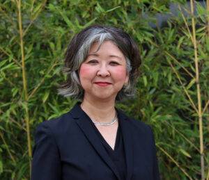
Aki Ishida, an associate professor and interim associate director of the School of Architecture at Virginia Tech, has been named director of the College of Architecture and Graduate School of Architecture & Urban Design in the Sam Fox School of Design & Visual Arts at Washington University in St. Louis.
As director, Ishida will oversee the Sam Fox School’s architecture, landscape architecture and urban design programs. She also will hold the Sam and Marilyn Fox Professorship. Both appointments begin July 1.
“Aki is an accomplished architect and designer, a respected scholar and a dedicated teacher and mentor,” said Carmon Colangelo, the Ralph J. Nagel Dean of the Sam Fox School and the E. Desmond Lee Professor for Collaboration in the Arts. “She is fascinated by the ways social conditions can shape the built environment, and she has a long history of collaborating with artists, engineers and health-care professionals, among others.
“I am confident Aki will be an inspiring leader who will connect deeply with our community and advance the strategic goals of the school and university. We are proud to welcome her to the Sam Fox School,” Colangelo said.
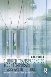
A licensed architect and widely admired educator whose work has been exhibited internationally, Ishida is author of “Blurred Transparencies in Contemporary Glass Architecture: Material, Culture, and Technology” (2020). In both her writing and design work, she investigates the temporal and impermanent aspects of architecture, emphasizing the ways buildings continue to change and evolve over the course of their lifespans.
“The physical constructs of a building are often understood to be firm, stable and long-lasting,” Ishida said. “But architecture’s mutable qualities carry equal importance. Questions of social justice, resource consumption, cultural symbolism and the spatial effects of buildings are inseparable from the decisions that architects make.”
A regular guest critic in the Sam Fox School, Ishida chaired the 2019 Fitzgibbon Charrette, a one-day sketch problem during which students selected and refined one of their studio drawings to highlight a particular phenomenon or experience. Ishida also chaired the 2020 Laskey Charrette, an intensive, weekend-long workshop that challenged students to experiment with modular assembly in cast concrete.
“It is an immense honor to lead the college with such talented and committed students, faculty and staff,” Ishida said. “I look forward to building upon its strengths to cultivate an inclusive, intellectually rigorous and forward-looking community of designers and scholars. Together, we can create a more sustainable, imaginative world, for and by a more diverse community of people.”
Ishida will succeed Heather Woofter, who led the Sam Fox School’s architecture programs from 2017 until summer 2023, when she was appointed dean of architecture at the University of Texas at Austin. Linda C. Samuels, a professor of architecture and chair of urban design, served as interim director for the 2023-24 academic year.

About Aki Ishida
Born in Tokyo, Ishida earned a Bachelor of Architecture in 1995 from the College of Architecture and Landscape Architecture at the University of Minnesota—Twin Cities. She began her career with Rafael Vinoly Architects in New York, as part of the core design team for a new Princeton University stadium, then earned a Master of Science in Advanced Architectural Design in 1998 from the Columbia University Graduate School of Architecture, Planning and Preservation.
Ishida spent four years with James Carpenter Design Associates in New York, where she gained experience in the artistic and technical applications of glass, then worked with acclaimed architect I.M. Pei as a full-time consultant on the Museum of Islamic Art in Doha, Qatar. In 2005, she co-founded Ishida/Crandall in New York and established Aki Ishida Architect in 2008. She is licensed in the states of New York and New Jersey and is a LEED-accredited professional.
Before joining the Virginia Tech faculty in 2012, Ishida led studios at the Rhode Island School of Design, The Pratt Institute, The Parsons School of Design and Konkuk University in Seoul, South Korea. Every summer since 2009, she has taught architecture courses in Columbia University’s Pre-College Program.
At Virginia Tech, Ishida led design studios; served as a senior fellow in the Institute for Creativity, Arts & Technology; directed the Intelligent Infrastructure for Human-Centered Communities destination area; and served as a faculty fellow in the provost’s office. Since spring 2022, she has served as interim associate director for the School of Architecture as well as for the School of Design, which includes Virginia Tech’s programs in industrial design, interior design and landscape architecture.
Since 2019, Ishida has been a co-principal investigator and design lead for “Medical Workspace: Information Ecosystem of Future Nurse Stations,” an interdisciplinary research project exploring how digital technologies, integrated into hospital intensive care units, might enhance communication and reduce clinician burnout. She also serves as co-PI for “Technology as Partner for Improving the Effectiveness of Teams of Clinicians,” funded by a National Science Foundation Future of Work at the Human-Technology Frontier: Core Research Development Grant.
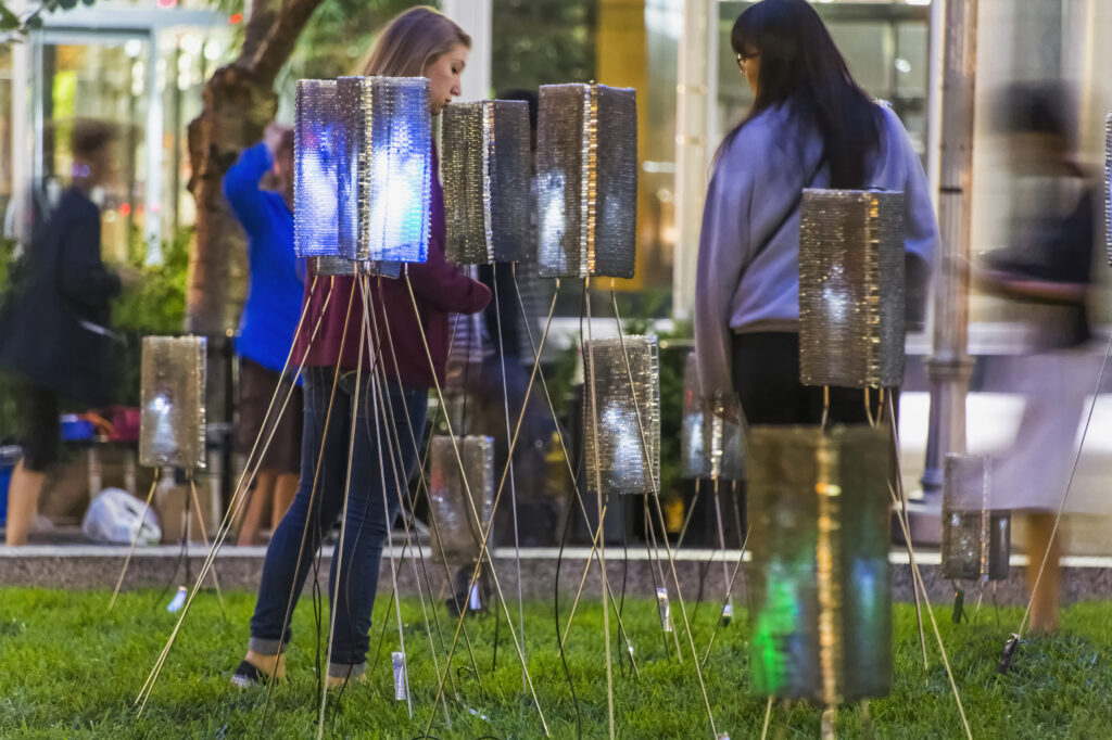
In 2023, Ishida won a Creative Achievement Award from the Association of Collegiate Schools of Architecture. She previously won the group’s New Faculty Teaching Award in 2017 and in 2016 was named one of 25 Most Admired Educators by DesignIntelligence. “Lantern Field,” an interactive audio-visual installation she led at the Smithsonian’s Freer Gallery in Washington, D.C., won a 2013 Architectural Lighting Design Award.
Ishida’s work has been supported by grants from Japan Foundation New York, the Graduate Kinne Traveling Fellowship from Columbia University, Stewardson Keefe LeBrun Travel Grant from the AIA New York Chapter, and fellowships from MacDowell and the Baer Art Center. She has served three times as a panelist for the National Endowment for the Arts grants and mentors faculty of color through the Dean’s Equity and Inclusion Initiative, a national group committed to nurturing academic diversity.
Comments and respectful dialogue are encouraged, but content will be moderated. Please, no personal attacks, obscenity or profanity, selling of commercial products, or endorsements of political candidates or positions. We reserve the right to remove any inappropriate comments. We also cannot address individual medical concerns or provide medical advice in this forum.
You Might Also Like

Latest from the Newsroom
Recent stories.
Epilepsy drug prevents brain tumors in mice with NF1
Molly Smith Metzler’s ‘Cry It Out’ in Hotchner Theatre April 18-21
Traube installed as Neidorff Family and Centene Corporation Dean of the Brown School
WashU Experts
Tremor a reminder that East Coast, Midwest earthquake threat is real
NASPA chair, WashU vice chancellor on the future of student affairs
How Key Bridge collapse could impact U.S. supply chains immediately, long-term
WashU in the News
As bird flu spreads in the US, is it safe to eat eggs? What to know about the risk to humans
Chlamydia vaccine shows promise in early trial
The government announced winners of a contest to tell real voices from deepfake audio

iPad Pro 2024 — 5 biggest expected upgrades
A pple hasn’t announced the iPad Pro 2024 , but rumors and reports suggest we could see it in May — just before the company’s big WWDC 2024 event.
Though all we've heard so far is rumors and hearsay, it’s a safe bet Apple will inevitably release an updated version of its premium tablet. This is especially true since we didn’t see any new iPads in 2023. The time is right for a new iPad Pro — which is rumored to receive significant upgrades along with the rest of the iPad line.
So far, we’ve heard that the iPad Pro 2024 will (finally) get an OLED panel and a landscape camera. The giant slate is also expected to pack an Apple M3 chip and sport a thinner design. We’ve also heard the Magic Keyboard peripheral is getting updated to help the iPad Pro function more like the best MacBooks .
Here are the 5 biggest rumored upgrades for the iPad Pro so far.
OLED display
Screen enthusiasts like our own Dave Meikleham have been clamoring for an OLED iPad Pro upgrade , and it seems it’s about to happen. Apple experts like Bloomberg’s Mark Gurman have said an OLED iPad Pro is coming for some time. Now, iPad Pro 2024’s biggest upgrade may have been confirmed by the iPadOS 17.5 beta .
9to5Mac dove into the beta’s code and discovered references to four unreleased iPad models. The models in question are labeled as iPad 16,3, iPad 16,4, iPad 16,5 and iPad 16,6. The site believes these are identifiers for the rumored iPad Pro 2024 and correspond to two different model sizes in Wi-Fi and cellular models.
The iPadOS 17.5 beta code also suggests those iPads will launch with an OLED display and that the two different-sized screens will come from different manufacturers. Regarding that last point, rumors say LG will supply the 12.9-inch panels of the larger iPad Pro while LG and Samsung will produce the 11-inch panels of the smaller variant.
An OLED panel would be a huge improvement over the current mini-LED panel in the 12.9-inch iPad Pro. According to Bloomberg reporter and Apple tipster Mark Gurman , the panel should be “crisper and brighter” and “reproduce colors more accurately.” An OLED panel would also place the iPad Pro’s display on more even ground with the Samsung Galaxy S9 Ultra which also sports the same panel technology.
Apple M3 chip
Another big upgrade for the iPad Pro 2024 is the inclusion of an M3 chip. This isn’t shocking considering how the current model has an M2 processor . That said, an M3-powered iPad Pro would make the 2024 model the most powerful iPad ever.
The Apple M3 chip utilizes TSMC’s 3nm process and brings big improvements in efficiency and speed. This is something we’ve seen firsthand when we tested and benchmarked the MacBook Pro 14-inch M3 , MacBook Air 13-inch M3 and MacBook Air 15-inch M3 . While gains between M2 and M3 aren’t earth-shattering, the leap from M1 to M3 is huge — with up to 60% faster performance.
Folks have been talking about the iPad Pro as a laptop replacement for years. The M2 iPad Pro brought us closer to that reality, but it’s possible the iPad Pro 2024 could see it come true. Of course, there are other factors involved, such as making iPadOS behave more like macOS, and improvements to the Magic Keyboard (more on that shortly). Regardless, an M3-powered iPad Pro would be a huge deal.
Landscape camera
iPads have historically had the front camera positioned on the short side of the display. That may have been fine when Apple first launched its tablets, but these days, people tend to use their tablets in landscape or horizontal mode. Having the front camera positioned on the tablet's right or left side (depending on how you hold or place it) isn't intuitive when it's horizontal.
Thankfully, a rumor suggests the iPad Pro 2024 could take a design cue from the iPad 10 in the form of a landscape-oriented camera on the front of the tablet.
Apple leaker Instant Digital posted an alleged image of the iPad Pro to the Chinese social media platform Weibo (via MacRumors ). The image in question shows that the iPad Pro 2024 will have its entire TrueDepth camera array to the right of the tablet, with the microphone remaining on the top but newly centered.
Back in January of this year, the iPadOS 17.4 beta code hinted that the iPad Pro’s Face ID sensors were being relocated from the top of the device when held in portrait, and to the top when held in landscape. "During Face ID setup, iPad needs to be in landscape with the camera at the top of the screen," the code read.
Since the iPad 10 now has its front camera up top in portrait mode, it wouldn’t be surprising if the iPad Pro followed suit.
Thinner design
The iPad Pro 2024 isn’t expected to receive major design changes to its overall profile. However, leaked iPad Pro CAD renders (via PocketNow ) suggest Apple plans to make its largest tablet thinner than previous models.
According to rumors, the 11-inch iPad Pro 2024 will be 0.20 inches thick compared to the 0.23 inches of the current model. The 12.9-inch iPad Pro is expected to drop from 0.25 to 0.19 inches thick. That might not seem like much, but it could make the giant tablets easier to hold for longer periods.
This ties back to the rumored OLED display. OLED screens are inherently thin so it makes sense the new iPad Pro will be thinner as a result. This should also affect the tablet’s weight. Right now, the 11-inch iPad weighs just a bit over 1 pound while its bigger 12.9-inch counterpart can weigh as much as 1.5 pounds. A reduced weight would also make it easier to hold the iPad Pro for longer.
Upgraded Magic Keyboard
An Apple Magic Keyboard for iPad Pro is an essential peripheral if you use the tablet for work or simply don’t like typing on the tablet's on-screen digital keyboard. We haven’t seen any major changes to the Magic Keyboard in quite some time, but it seems it’s finally getting one just in time for the iPad Pro’s release.
Mark Gurman reports that the Magic Keyboard will sport a look that’s reminiscent of an Apple laptop. To that end, the peripheral will reportedly get an aluminum finish to give it the appearance of a MacBook. It will also have a larger touchpad that’s more akin to an Apple notebook. This would further realize the dream of making the iPad Pro a laptop replacement I mentioned above.
Speaking of iPad Pro peripherals, rumors say the Apple Pencil 3 is launching this year. Based on what 9to5Mac discovered in the aforementioned iPadOS 17.5 beta code, there’s evidence of a new “squeeze” feature for an as-yet-unreleased Apple Pencil . This could very well be the rumored Apple Pencil 3. The site also suggests this stylus could feature interchangeable magnetic tips. The Apple Pencil 3 could also work with the Vision Pro headset.
More from Tom's Guide
- WTF? The OLED iPad Pro could get an obscene price hike
- iPad Air 6 tipped to get OLED upgrade after iPad Pro
- iPhone 16 Pro Max — 7 biggest rumored upgrades
This article may contain affiliate links that Microsoft and/or the publisher may receive a commission from if you buy a product or service through those links.

IMAGES
VIDEO
COMMENTS
Graduate students also will have a "project-based" option for the MS degree, or stackable certificates at MS level, that will prepare them to be workforce-ready upon graduation. Students will design, fabricate, and test their own semiconductor chips through innovative partnerships with industry.
Research in chip design and architecture comprises a multidisciplinary group of researchers exploring theoretical, experimental, and applied aspects of silicon chip design, computer architecture and novel device technologies that may replace traditional CMOS transistors as the basic unit of computation. The research in this space includes ...
Dr. Mehdi Saligane, a leader in the open-source chip design community, was among the first researchers to fabricate a successful chip as part of Google's multi-project wafer program. ... PhD student Trevor Odelberg is looking to enable long range, highly reliable, and low-power cellular IoT devices that one day can run entirely on harvested ...
Machine learning tools are used to greatly accelerate chip layout design, by posing chip floorplanning as a reinforcement learning problem and using neural networks to generate high ...
The modern world runs on semiconductor chips. They form the backbone of the entire computing and electronics industries and almost any product that plugs into a wall has at least one semiconductor chip (likely, many more) inside. A worldwide shortage of semiconductors â tried to buy a car lately? â caused by pandemic-induced supply chain disruptions has brought into sharp focus the need for ...
The PhD in Design and Process for Semiconductor System-on-Chip at HUST is a 3 year PhD Program for international students taught in English. The incessant march of Moore's Law, which has enabled exponential growth in the number of transistors in integrated circuits, has culminated in System-on-Chips (SoCs) where many functions of an ...
With the support of Apple, Nikolić, fellow professors Kris Pister and Ali Niknejad, and graduate student instructors Dan Fritchman and Aviral Pandey led 10 undergrads, five master's students and four Ph.D. candidates through the design and successful tape-out of a novel chip within the span of a single semester.
Jiang Hu, PhD Professor and Co-director of Graduate Programs in the Department of Electrical & Computer Engineering at Texas A&M University. ... As chip design gets cheaper and more efficient, more chips will be available to help boost the power of AI and ML computing. Currently, large language models (LLMs) like ChatGPT need to be trained, and ...
The University of Michigan is part of a growing movement to make integrated circuits (IC) or chip design more accessible by providing open-source process design kits (PDKs), EDA tools, and building blocks. Chips developed from these design kits are now also invited to be fabricated at no cost to the developer thanks to a cooperative research ...
Speaking of economics - it costs a lot to design a chip and a small chunk to make a chip. It costs a lot to design software but to make a copy is almost free. Silicon is bound by economics of traditional manufacturing - gross margins vs net margins - whereas the gross margin of software can be almost 100%.
Dr. Mehdi Saligane, a leader in the open-source chip design community, was among the first researchers to fabricate a successful chip as part of Google's multi-project wafer program. ... PhD student Trevor Odelberg is looking to enable long range, highly reliable, and low-power cellular IoT devices that one day can run entirely on harvested ...
SHARE. Brain-Inspired Chip Design Stands the Test of Time. The amount of time and energy spent shuttling data from one location to another—writing results, storing them, and retrieving them to perform calculations—consumes the major share of a computer's time and energy. In fact, the data traffic jams that occur as information flows from ...
"Chip design is getting more complex, with increasing costs and longer development cycles," said UCLA electrical and computer engineering professor Dejan Markovic, PhD. "PyGears addresses these challenges by adopting a modular build of hardware out of reusable components, which are built by a community of like-minded contributors.
Learn next-level VLSI design skills for top Silicon Valley companies in this five-course certificate program at UCSC Silicon Valley Extension. We work closely with industry partners to bring you the latest technology and best practices in this Silicon Chip & Semiconductor Engineering professional certificate program. Learn core design skills practiced at top companies in the Valley from our ...
After one semester into my MS, a professor who does chip design offered me a PhD role if I wanted to stay an extra 1.5 years. This role would allow me to be fully funded and get direct experience in a tape out. There is funding for 2 tape-outs (the first one would be more of an experimental chip with the second being a final design).
Unique Semiconductor Chip Design Course Attracts Canadian Graduate Students. MONTREAL, QC - May 19, 2021: A unique course for designing integrated semiconductor chips conceived and organized by Gayathri Singh, Team Leader for Microelectronics at CMC Microsystems is a hot ticket with graduate students at Canadian universities.
A PhD is rarely useful in industry - chip design in general is somewhat an exception - analog design is a subset of chip design where it's a serious exception, and a PhD is seen quite highly and can come in very useful. Now of course, useful as it might be, the opportunity cost of getting a PhD versus the extra pay (if any) for having one do ...
With worldwide semiconductor revenue reaching $450 Billion in 2020, there is a need to design and produce highly efficient and specialized chips. The Post Graduate Certificate in VLSI Design enables professionals to develop VLSI chip designing capabilities that can power new-age technologies like AI, IoT, VR, mobility, cloud, and analytics.
SK hynix Inc. announced Wednesday (April 3) that it plans to invest close to $4 billion to build an advanced packaging fabrication and RD facility for AI products in the Purdue Research Park. The development of a critical link in the U.S. semiconductor supply chain in West Lafayette marks a giant leap forward in the industry and the state.
You have highlighted how PhD training assessment has stagnated, despite evolving educational methodologies (see Nature 613, 414 (2023) and Nature 627, 244; 2024). In particular, you note the ...
To be honest, both these fields can actually also lead away from a chip design career as well due to the fringe nature of the applications. Having said that, I think optical interconnects could lead to some challenging future design problems but the NVM research could remain confined to the field of device research. true.
The Alphabet subsidiary said the new TPU v5p chip is built to run in pods of 8,960 chips, and can achieve twice the raw performance as the prior generation of TPUs. To help ensure the pod runs at ...
MFA Thesis Exhibition. May 30 - June 9. RailSpur. Opening Reception: Thursday, May 30, 7:30-9:30pm. The Division of Art presents the work of the 2024 Master of Fine Art (MFA) graduates: David Braun, Free Bàssïbét, Rachel Dorsey, Amara Eke, Ren Han, Michael Hong, Ali Meyer, and Kevin Phan. Closing reception on June 6 (first Thursday) from 6 ...
Aki Ishida, an associate professor and interim associate director of the School of Architecture at Virginia Tech, has been named director of the College of Architecture and Graduate School of Architecture & Urban Design in the Sam Fox School of Design & Visual Arts at Washington University in St. Louis.
The group's work is integrated photonics, but we design analog circuits primarily and this is my interest, in addition to mixed-signal design circuits. The lab is very new, part of the first cohort and we've just submitted our first tapeouts. I came into graduate school intending to go into academia, but have lost all interest in this.
Park City High School graduate Camden Woll and his team of University of Utah graduate students placed first in the Utah Real Estate Challenge on April 11. The UREC is a statewide competition that the Ivory-Boyer Real Estate Center hosts annually with a grand prize of $20,000. Awards were presented at the Grand America Hotel Luncheon.
According to rumors, the 11-inch iPad Pro 2024 will be 0.20 inches thick compared to the 0.23 inches of the current model. The 12.9-inch iPad Pro is expected to drop from 0.25 to 0.19 inches thick ...