Accessibility Links
- Skip to content
- Skip to search IOPscience
- Skip to Journals list
- Accessibility help
- Accessibility Help
Click here to close this panel.
As a society-owned publisher with a legacy of serving scientific communities, we are committed to offering a home to all scientifically valid and rigorously reviewed research. In doing so, we aim to accelerate the dissemination of scientific knowledge and the advancement of scholarly communications to benefit all.
Materials Research Express supports this mission and actively demonstrates our core values of inclusive publishing and trusted science . To find out more about these values and how they can help you publish your next paper with us, visit our journal scope .
Purpose-led Publishing is a coalition of three not-for-profit publishers in the field of physical sciences: AIP Publishing, the American Physical Society and IOP Publishing.
Together, as publishers that will always put purpose above profit, we have defined a set of industry standards that underpin high-quality, ethical scholarly communications.
We are proudly declaring that science is our only shareholder.

Quantum dots: an overview of synthesis, properties, and applications
Kushagra Agarwal 1 , Himanshu Rai 1 and Sandip Mondal 1
Published 12 June 2023 • © 2023 The Author(s). Published by IOP Publishing Ltd Materials Research Express , Volume 10 , Number 6 Citation Kushagra Agarwal et al 2023 Mater. Res. Express 10 062001 DOI 10.1088/2053-1591/acda17
Article metrics
16603 Total downloads
Share this article
Author e-mails.
Author affiliations
1 Department of Electrical Engineering, Indian Institute of Technology Bombay, Mumbai 400076, India
- Received 24 March 2023
- Revised 16 May 2023
- Accepted 30 May 2023
- Published 12 June 2023
Peer review information
Method : Single-anonymous Revisions: 2 Screened for originality? Yes
Buy this article in print
Quantum dots (QDs) have sparked great interest due to their unique electronic, optical, and structural properties. In this review, we provide a critical analysis of the latest advances in the synthesis, properties, and applications of QDs. We discuss synthesis techniques, including colloidal and hydrothermal synthesis, and highlight how the underlying principles of these techniques affect the resulting properties of QDs. We then delve into the wide range of applications of QDs, from QDs based color conversion, light-emitting diodes and biomedicine to quantum-based cryptography and spintronics. Finally, we identify the current challenges and future prospects for quantum dot research. By reading this review, readers will gain a deeper understanding of the current state-of-the-art in QDs research and the potential for future development.
Export citation and abstract BibTeX RIS
Original content from this work may be used under the terms of the Creative Commons Attribution 4.0 licence . Any further distribution of this work must maintain attribution to the author(s) and the title of the work, journal citation and DOI.
Abbreviations
1. introduction.
QDs are tiny semiconductor nanoparticles [ 1 , 2 ] just a few nanometers in size (ranging from a few nanometers to tens of nanometers) which possess one of the most important properties of quantum confinement [ 3 ]. Onyia et al [ 4 ] theoretically studied the effect of quantum confinement on QDs using particles in a box model. More generally, when a system has one or more dimensions small enough to affect its electronic density of states then the system is said to be confined. And accordingly, we have QDs in which electrons are confined in all directions which leads to larger oscillator strength for electronic transitions that can be used to make a wide range of electronic devices, including solar cells, LEDs, and transistors.
QDs have different properties than bulk materials like - size, as due to the small size of the QDs they have a high surface-to-volume ratio making them highly reactive (or active) whereas bulk materials are larger in size. QDs have discrete quantized energy levels in the density of states having (delta) like function shown in figure 1 [ 5 ] rather than a continuous range of energy levels like in bulk materials.

Figure 1. Schematic illustration of the changes in the density of states (DOS) where (A) Bulk material, (B) 2D, (C) 1D, (D) 0D.
Download figure:
At this scale, the electronic and optical properties of the material begin to deviate from those of the bulk material such as sharp absorption and emission spectra. In addition to this, QDs have an impressive ability to tune their band gap which can be effectively controlled by regulating the size of the QD. Also, several other methods of tuning the bandgap by alloying the core of the QDs were also demonstrated [ 6 , 7 ]. This property is not found in bulk materials. Carefully controlling these properties makes QDs highly attractive for a wide range of applications in areas such as sensing [ 8 ], medicine i.e. light-based therapeutics and diagnosis [ 9 , 10 ], biotechnology [ 11 ], optoelectronics, and materials science [ 12 ].
Different types of QDs have been used depending on types of applications and their unique properties. Early in the 1980s, the history of QDs may have been established when researchers first started looking into the characteristics of semiconductor particles small enough to display quantum confinement. Alexey Ekimov's research in 1981 is widely regarded as the first recorded experimental observation of quantum confinement in semiconductor nanocrystals, which are currently known as QDs. Using a chemical synthesis technique, Ekimov and his team produced cadmium selenide (CdSe) nanocrystals within a glass matrix, and they discovered that the nanocrystals' optical characteristics varied significantly from those of bulk CdSe, which classical physics could not explain [ 13 ]. In the following years, researchers began to explore other semiconductor materials for use in QDs, including cadmium telluride (CdTe), indium arsenide (InAs), and indium phosphide (InP). Each of these materials has unique properties because they have different band gaps that makes them well-suited for wide applications. For example, QDs based on the I-III-VI compositions, such as copper indium sulfide (CuInS 2 ) and zinc sulfide (ZnS), are considered excellent alternatives to cadmium-based QDs for biomedical applications due to their lower toxicity. Moreover, in addition to being more biocompatible, Ag-In-S QDs [ 14 ] exhibited great potential for light absorption and emission. They also have a long photoluminescence (PL) lifetime and high quantum yields
CdSe is a good choice for use in optoelectronics [ 15 ] and bioimaging [ 16 ], while CdTe and InAs are used in solar cells and infrared detectors. These QDs can be grown from both organic and inorganic materials. QDs come in various structures, including the new Ternary I-III-VI type, which is a safer alternative to heavy metal-containing QDs. Copper indium sulfide (CIS) structures [ 17 ], with atoms arranged in a crystal lattice, are crucial for modern technologies. By altering the size of CIS QDs, their band gap can be adjusted, making them highly adaptable for use in solar cells [ 18 ] and LEDs [ 19 ], leading to more efficient devices with greater color variety. Additionally, CIS QDs are stable and easily synthesized, making them a promising material for applications such as biophotonics. Incorporating QDs into matrix structures creates nanocomposites with unique properties, improved stability, and enhanced mechanical properties. For instance, using CdZnTe QDs in a CaCO 3 matrix [ 20 ] results in excellent photostability when compared to pure CdZnTe QDs. Additionally, the nanocomposite exhibits good processability, making it a promising material for various applications.
Perovskite QDs are a promising class of semiconductor nanoparticles that have gained significant attention in recent years due to their superior optical and electronic properties [ 21 ]. PQDs have high photoluminescence quantum yields, narrow emission bandwidths, and excellent color purity, making them a desirable alternative to conventional QDs. They also have the potential to be used in various optoelectronic devices, such as LEDs, solar cells. The development of PQDs has great potential to revolutionize the field of optoelectronics.
More recently, researchers have begun to investigate the use of other types of nanostructured materials, such as carbon nanotubes and graphene, as QDs. These materials have unique electronic characteristics and highly tunable Photoluminescence (PL) properties. This versatility makes them ideal for use in various fields, such as optoelectronics, sensing, and energy storage [ 8 , 22 ]. Ongoing research is being conducted to find alternatives to heavy metal-containing and heavy metal-free emitters due to concerns such as toxicity and environmental impact. One such alternative is III-V QDs, particularly InP [ 23 ], which are being widely used in the development of next-generation displays.
Several growth methods were developed during the period to grow these nanoparticles suitable for different applications [ 24 , 25 ]. However, there are different challenges or trade-offs faced by different applications because of the formation of these QDs for example inorganic QDs are toxic but show high stability against external parameters like temperature and humidity. On the other hand, organic QDs are non-toxic but can highly be affected by temperature, pressure, and humidity. Here, the cost and complexity of the synthesis process play a crucial role depending on the application requirements. Inorganic QDs [ 26 ] can be expensive to produce and may require high temperatures and pressures for synthesis while organic QDs are relatively inexpensive and abundant.
It's worth mentioning that researchers are working to overcome the toxicness of QDs [ 27 ] and trying to find new ways to use them in various applications. For example carbon QDs are showing great bio-compatibility to use in biosensing applications [ 8 ]. In this overview, we provide a brief examination of the structure, characteristics, fabrication, and various applications of QDs.
2. Structure of QDs
2.1. quantum vs bulk properties.
A close arrangement of atoms or molecules is following the quantum rules referred to as QDs. In most cases, QDs consist of a core made of a semiconductor material and a shell made of a separate material that serves as a surface passivation layer. Different sizes and shapes of the core and shell are possible, and their qualities can be adjusted to fit particular applications. For instance, spherical QDs differ from rod- or disk-shaped QDs in their optical and electrical characteristics. The electrical and optical characteristics of QDs are determined by its core, while its stability and interactions are governed by the shell. The structure of the QDs are responsible for electrical and optical properties required for a specific application.
Quantum confinement, as previously established, is the characteristic that sets QDs apart from other bulk materials. Researchers have intensively studied the impacts of quantum confinement on semiconductor QDs [ 28 – 36 ]. When a QD follows the quantum confinement effect, the motion of excitons has been constrained to a quantized space leading to a quantum confinement giving QDs their distinctive optical and electrical properties. To achieve quantum confinement Bohr condition needs to be satisfied. This indicates the size of the nanoparticle must be smaller than the corresponding exciton Bohr radius [ 37 ].
One of the key differences between QDs and bulk materials is the size-dependent energy bandgap. In bulk materials, the bandgap is a property of the material itself and does not change with size. However, in QDs as shown in figure 2 , the bandgap is inversely proportional to the size of the QD. The size of the QDs is important because it determines the strength of the quantum confinement effect. Smaller QDs exhibit stronger quantum confinement and have higher energy levels than larger QDs. Controlling the size of the QD during growth is a significant factor in the advancement and creation of new devices and their applications [ 36 ]. This size-dependent bandgap leads to a broad range of optical properties, including tunable absorption and emission spectra etc

Figure 2. Schematic diagram showing energy band structures in bulk material and quantum nanostructure.
For example the bandgap of CsPbBr 3 QDs increases from 2.3 to 2.5 eV with distinct blue shifts in the PL spectra when particle size decreases from 8.5 to 4.1 nm, according to Butkus et al 's research [ 38 ]as shown in figure 3 .

Figure 3. Experimental versus theoretical size-dependent bandgap energy of CsPbBr 3 . Reprinted with permission from [ 38 ]. Copyright (2017) American Chemical Society.
2.2. Optical properties of QDs
Due to their small size and the quantum confinement effect, QDs exhibit unique optical characteristics. Currently, there is a significant amount of research being conducted on core-multishell QDs. The structure consists of numerous shells made of various materials surrounding a central core made of a single material. By selecting different materials, the size and composition of the QDs can be altered, resulting in distinctive optical and electronic properties [ 39 ]. These different structures result in high photoluminescence quantum yields (PL-QY). The stability of the QDs is enhanced by the additional protection that the various layers offer the core. The core is typically made of a material with a direct bandgap, such as cadmium selenide (CdSe), while the shells are made of a different material, such as zinc sulfide (ZnS), that has a wider bandgap [ 40 ]. This multi shell design results in unique optical properties, such as broad and tunable photoluminescence and improved stability compared to traditional single-component QDs.
linkov et al proposed [ 41 ] a core-multishell QDs made of CdSe/ZnS/CdS/ZnS as shown in figure 4 as a substitute of a single shell. The multilayer shells have several advantages over single layered shells. For example, by adding different numbers of layers of shell increases, quantum yields have been achieved. These properties make core-multishell QDs useful in various applications such as LEDs, solar cells, and bio-imaging.

Figure 4. (a) Structure of a core-multishell QD (b) Photoluminescence spectra of QDs with different shell thickness. Reproduced from [ 41 ], with permission from Springer Nature.
The optical properties of QDs are an important area of research, as they are related to the size, shape, composition, and surface chemistry of the dots. The optical properties of QDs can be tuned in many ways such that they can be taken as an advantage in wide applications. One such property shown in figure 5 is their broad and continuous excitation profile, which means they can be effectively excited at any wavelength below 530 nm. This is in contrast to organic dyes like rhodamine 6 G [ 42 ], which have a limited excitation range and a wide emission spectrum. Additionally, QDs have almost symmetrical and narrower emission spectra compared to organic dyes. These properties make QDs more versatile and efficient in a wide range of applications.

Figure 5. Excitation (a) and emission (b) profiles of rhodamine 6 G and CdSe QDs. Reprinted from [ 42 ], Copyright (2002), with permission from Elsevier.
Other QDs such as inorganic perovskite QDs (PQDs) are a type of nanomaterials that have gained attention in recent years due to their unique optical properties. They have a high quantum yield which is the fraction of absorbed photons that are emitted as photoluminescence. This property makes PQDs efficient light emitters and is important for applications where high light output is required. Strong and focused PL light emissions are seen from inorganic perovskite QDs. Inorganic perovskite QDs (PQDs) can exhibit a photoluminescence quantum yield (PLQY) greater than 99% without the need for surface passivation through the use of wide-bandgap epitaxial shells, unlike conventional semiconductor QDs such as CdSe, CdS, or PbS [ 43 ].
To overcome the limitations of the structural properties of QDs various compositional types of QDs including doped QDs are utilized. These QDs contain impurities or dopants, typically metal or non-metal elements, incorporated into their core or shell structure, which introduce new electronic states into the QD, thereby modifying its properties such as bandgap, charge carrier dynamics, and emission wavelength. The dopants can be carefully controlled to tailor the QD's properties for specific applications. Doped QDs have been found to enhance the performance of optoelectronic devices such as light-emitting diodes by improving their efficiency and stability. Another class of semiconductor QDs that is alloyed semiconductor QDs have emerged as a significant area of research due to their unique optoelectronic properties. These QDs consist of a single crystalline structure made up of two or more different materials with varying sizes [ 44 ]. The composition and size of these constituent materials are controlled to modify the properties of the resulting QD for specific applications. For example, To adjust the emission of CdSe QDs, alloying them with ZnSe [ 45 ] is a common approach as it is challenging to control their emission solely through the quantum confinement effect. This method enables the tuning of the bandgap energy and allows for more precise control over the emission wavelength of the QDs. Alloyed QDs exhibit improved luminescence efficiency, thermal and photo stability, and reduced sensitivity to external factors like moisture and temperature.
2.3. Surface passivation
The surface of the QD can significantly affect the electrical and optical properties of QDs. Hence surface passivation is necessary for QDs. Device efficiency and stability can suffer due to surface-induced defects and trap states that impact carrier recombination. The size and shape of QDs can also be influenced by the surface. In order to address these problems, surface passivation is used to 'heal' the surface of the dot. The development of different ligand structures which covalently bonded with the QDs in turn act as a protective coating or capping layer. This procedure increases the stability and effectiveness of the device. It further lowers the density of defects and trap states and can help to maintain the size and shape of QDs. Overall, the passivating layer must be able to protect the surface from environmental degradation. Numerous studies have investigated how surface passivation affects a material's optical and electrical characteristics. Improving luminescence qualities by preventing non-radiative recombination and minimizing defect states. Although ligands help ensure that QDs are in a stable phase, having too many capping ligands on the surface of the QDs potentially makes charge transport difficult which impacts the optoelectronic properties of Light-emitting Diodes (LEDs) [ 46 ]. The choice of passivating layer is important to obtain high performance and stability of the QDs. High electron mobility, a low surface recombination rate, and strong chemical stability are all desirable qualities in a passivating material. There are several different methods that have been proposed for the surface passivation of QDs, including the use of organic ligands that act as a capping agent shown in figure 6 [ 47 – 49 ], inorganic coatings, and self-assembled monolayers.

Figure 6. Schematic illustration of organic capped Quantum dot.
Jung et al reported the creation of high-quality QDs using environmental friendly electrically active metal chalcogenide complex ligands (Sn 2 S 6 4− , Sn 2 Se 6 4− , and In 2 Se 4 2− ). This ligand helps to stabilize the QDs in polar solvents such as formic acid, dimethylformamide (DMF), N-methylformamide, and dimethyl sulfoxide (DMSO). This method showed improvement in the stability and charge transport in devices [ 50 ].
3. Synthesis and characterization of QDs
Synthesis and characterization of QDs refer to the process of creating and studying the properties of QDs. Synthesis involves the methods used to create QDs, such as colloidal synthesis, chemical vapor deposition (CVD), and physical vapor deposition (PVD). Characterization involves studying the properties of the QDs, such as size, shape, composition, and optical properties. This can be done using techniques such as transmission electron microscopy (TEM), x-ray diffraction (XRD), and spectroscopy (such as absorption, photoluminescence, and Raman). The aim is to understand the relationship between the synthesis conditions and the resulting QD properties. Finally, it has been discussed the optimization of synthesis conditions to produce high-quality QDs with desired properties for different applications.
3.1. Colloidal synthesis
Colloidal synthesis is a widely used method for producing QDs, and the high-temperature version is particularly effective. Murray, Norris, and Bawendi first proposed this chemical technique in 1993 to produce QDs [ 49 ]. The process involves dissolving metal ions or organometallic compounds, known as precursors, in a solvent, and then subjecting them to various chemical or physical treatments to create the desired QDs. The primary advantage of this synthesis method is its ability to produce QDs of varying sizes with great ease, making it highly tunable [ 51 , 52 ].
One of the popular techniques of colloidal synthesis is the 'Hot Injection Method'. In this a precursor solution containing the appropriate elements is quickly injected into a hot, high-temperature reaction mixture. As a result, the precursors react quickly to generate QDs, which quickly cool and solidify. By adjusting the type, the concentration of the precursor, reaction time, and temperature during synthesis, the size and composition of colloidal QDs can be controlled [ 53 ]. This approach allows for the efficient and rapid synthesis of high-quality QDs of homogeneous size distribution (shown in figure 7 ) in large quantities.

Figure 7. Colloidal QDs, The solution-processed synthesis resulting in colloidal nanocrystal inks, self-assembly of QDs with highly monodispersed size and shape leads to long-range ordered superlattices. Reproduced from [ 54 ], with permission from Springer Nature.
The colloidal QDs is particularly useful for the synthesis of inorganic QDs, such as CdSe or CdS and halide perovskites [ 55 ]. Irshad Ahmed et al as shown in figure 8 [ 56 ]demonstrated the synthesis of CdSe QD in the 'Hot Injection Method' versus 'Room temperature method'. It was noted that the smallest QD created using the HI-method had a size of 2.5 nm. Only QDs with a 3.3 nm size could be manufactured using the RT approach. The effect of synthesis protocol on the fluorescence property was also studied in figure 9 and compared with the RT method. The HI-QDs demonstrated high photochemical stability, indicating their potential for use in the development of optoelectronic devices. This synthesis method offers several advantages over other methods, including precise control on the size and shape of the QDs, high purity, and low defect density. The process is relatively straightforward to scale up, and it can be used to produce a broad range of different QD types. As a result, this method has been extensively used in recent years to produce high-quality QDs for various applications.

Figure 8. Under bright light and ultraviolet (UV) illumination, the two procedures for CdSe quantum dot synthesis. Reprinted from [ 56 ], Copyright (2016), with permission from Elsevier.

Figure 9. Fluorescence spectra of the Quantum dot samples obtained from Hot Injection (HI) and Room Temperature (RT) synthesis. Reprinted from [ 56 ], Copyright (2016), with permission from Elsevier.
Significant amount of data has been produced on QDs by experimentalists and theorists. Machine learning methods used to analyze this data, identify patterns, and accurately make the predictions. For example, Krishnadasan et al developed an autonomous black-box system to control the synthesis of CdSe QDs in a microfluidic reactor [ 57 , 58 ]. By utilizing a global search algorithm SNOBFIT, they discovered the optimal injection rate and reaction temperature, which increased the emission intensity at a specific wavelength [ 59 ].
New precursors, capping agents, and synthetic techniques have recently been developed in colloidal synthesis, allowing exact control over the QDs' size, shape, and makeup. For instance, using PEG or DHLA (dithiol-PEG-dithiol) as ligands for capping can result in creation of extremely monodisperse QDs with precise size and shape.
Aqueous-based synthesis is one of the cost-effective and environmentally friendly methods to synthesize stable colloidal QDs. This method involves a solution-based chemical reaction using precursor solutions and a base to trigger nucleation and growth of QDs in a colloidal solution, without the use of toxic solvents or high temperatures. core–shell QDs can be easily grown using this technique to produce highly luminescent QDs. Reza Sahraei et al [ 60 ] have developed a growth-doping strategy for the one-pot synthesis of water-soluble dual-doped Ag,Ni:ZnCdS/ZnS core/shell QDs, which is a novel approach.
3.2. Hydrothermal synthesis
The hydrothermal method is a simple and low-cost method for the preparation of QDs with well control on size and shape. In this method, a precursor solution containing metal ions and ligands is placed in a sealed container and heated under high pressure in a water bath. As the temperature and pressure increase, the solution becomes supersaturated, hence nucleation of the QDs occurs. The size and shape of the QDs can be controlled by varying the reaction parameters such as temperature, pressure, and reaction time. One of the advantages of hydrothermal synthesis is that it allows the synthesis of QDs at relatively low temperatures compared to other methods such as high-temperature furnaces or molecular beam epitaxy. Hydrothermal synthesis is a method for synthesizing QDs in which a precursor solution is heated in a sealed vessel (typically a high-pressure autoclave) at high temperatures and pressures.
Zhu et al presented a straightforward hydrothermal method for producing uniform, mono dispersed SnO 2 QDs with a narrow diameter range in their study (2.3 to 3.1 nm). The key to the hydrothermal technique described here is to use the hydrazine hydrate, or N 2 H 4 H 2 O, which serves as both an alkali and a ligand to coordinate with the Sn ions and create a complex cluster [ 61 ].
The hydrothermal method offers an easy way to create high-quality cysteamine-stabilized CdTe QDs, whose quantum yield (QY) can reach 19.7% under ideal conditions reported by Wei-haiYang et al [ 62 ]. The growth rate is faster than the aqueous method in which the CdTe QDs were grown at 220 °C for 20 min. During this time the absorbance peak changed from 490 nm to 640 nm shown in figure 10 and the mean particle sizes changed from 2 nm to 4 nm.

Figure 10. Change in the absorption and photoluminescence spectra over time for CdTe QDs covered with a CA cap. Reprinted from [ 62 ], Copyright (2008), with permission from Elsevier.
Hydrothermal synthesis allows for the synthesis of QDs such as carbon QDs (CQDs) doped in nitrogen forming NCQDs. This has successfully proven to be a good imaging agent that can be beneficial for certain applications such as bioimaging [ 63 ]. Because of its straightforward operating conditions such as low energy requirement, and inexpensive apparatus, hydrothermal synthesis is thought to be the most accessible approach. The basic schematic illustration of this synthesis approach is given in figure 11 .

Figure 11. Schematic illustration of the synthesis of nitrogen-doped carbon QDs (N-CQDs) by a hydrothermal treatment approach.
CQDs created using this synthesis technique, however, frequently have a poor fluorescence quantum yield (QY) of less than 10% [ 64 ]. Doping with nitrogen has been demonstrated to be a successful method of enhancing these qualities in order to counteract this effect [ 65 ]. The numerous benefits of CQDs can be retained by nitrogen-doped CQDs (N-CQDs), but they can also overcome this drawback. In addition, the carbon sources utilized to create N-CQDs have a significant impact on their QY and optical properties. It can be observed from figure 12 that the fluorescence emission intensity of N-CQDs is stronger than that of CQDs solutions with the same concentration. Peng wu et al [ 66 ] synthesized the N-CQDs by the hydrothermal method and it showed that these N-CQDs have been demonstrated to be effective as a fluorescent probe for detecting Fe 3+ ions in highly acidic environments. This is due to their superior fluorescence emission properties that result in good selectivity and sensitivity to Fe 3+ ions.

Figure 12. (a) UV–vis absorption spectra of NCQDs and CQDs irradiated at 360 nm. (b) Fluorescence emission spectra of NCQDs and CQDs excited at 360 nm. Reproduced from [ 66 ] with permission from the Royal Society of Chemistry.
Hydrothermal synthesis also has few limitations. The high-pressure and temperature conditions required can be challenging to control, which can make it difficult to obtain highly uniform and monodisperse QDs [ 67 ]. Hydrothermal process is relatively cost-effective, as it only requires a few precursor materials, an autoclave, and an oven, while reflux methods often require a Schlenk line and an oxygen-free medium, with the need for multiple precursor injections during synthesis.
Some recent advances in the hydrothermal synthesis of QDs include the development of new precursors and surfactants that can be used to improve the size and shape control of the QDs. Additionally, researchers have been exploring the use of alternative solvents such as ionic liquids and supercritical fluids [ 68 ], which can offer improved solubility of precursors and better control over the reaction conditions and can result in high quality and uniform QDs with a narrow size distribution.
3.3. Biomimetic synthesis
Biomimetic synthesis of QDs refers to a process of synthesizing QDs using biological materials. In this process, the growth and self-assembly of QDs are mimicked based on the mechanisms and principles found in biological systems. The use of biomimetic techniques in the growth of QDs has several advantages over traditional synthetic methods. High temperatures, harsh chemicals, and high pressures are frequently needed in these conventional synthetic processes in order to grow the QDs. Large size and uneven distribution, as well as flaws and impurities may occur under these circumstances. This leads to an impact on the optical and electrical capabilities of QDs. However, the development of 'green' biomimetic mineralization technology makes the production of (II-VI, IV-VI, and I-VI) QDs simpler. The use of enzymes, proteins, or microorganisms as catalysts can help to reduce the use of harsh chemicals and high temperatures, making the synthesis process more environmentally friendly and biocompatible [ 69 ]. Additionally, the use of Biomolecules such as proteins, enzymes, and DNA are used to stabilize the QDs and control their size, shape, and surface properties. These biomolecules help to reduce the formation of defects and prevent the aggregation of QDs, ensuring that they remain well-dispersed and stable. The synthesis process typically involves the introduction of the precursors for the QD formation into a reaction medium containing the stabilizing biomolecules and the biotemplate. The reaction medium is then subjected to specific conditions, such as temperature, pH, and time, to allow the QDs to grow. The resulting QDs are then separated from the reaction medium and purified, if necessary. Overall, biomimetic synthesis is an important approach for producing high-quality QDs for various applications in optoelectronics, energy, biology, and medicine.
Li et al [ 70 ] discovered a straightforward, one-pot, environmentally friendly method to make CdSe QDs using lysozyme (Lyz) and bovine serum albumin (BSA) as the respective biotemplates. Bacterial cells were then marked with the BSA-functionalized CdSe QDs that had been produced. And it was determined that lysozyme's biological activity persisted after CdSe was formed, which is essential for creating fluorescent nanoprobes with biological function.
A work done by Arriaza et al [ 71 ] where they demonstrated a biomimetic approach shown in figure 13 for synthesizing CIS (CuInS 2 ) QDs, which proved to be a green chemistry approach that retains some biological characteristics in the chemical process. CIS nanoparticles are the top choice for numerous technical applications, including solar cells and biomedicine [ 72 ].

Figure 13. Overview of synthesis and characterization of CIS QDs. Reprinted from [ 71 ], Copyright (2021), with permission from Elsevier.
3.4. Other synthesis process
Rapid and easy synthesis techniques are crucial for scientists to conduct more precise experiments within a short period while minimizing heat release into the environment. Microwave-assisted synthesis [ 73 ] provides a rapid and easy alternative energy source that is widely used due to its control over the heating of materials. This method has proven to be effective for QD preparation, with several studies confirming its feasibility and potential. QD precursors are dissolved in a solvent and irradiated with microwaves in a reactor, resulting in the formation of QDs with a narrow size distribution and high crystallinity [ 74 ]. Microwave-assisted synthesis has many advantages over traditional synthesis methods [ 75 , 76 ], including shorter reaction times, reduced energy usage, and better product yields. It also provides accurate control over the size and shape of the QDs, which is crucial for many applications.
4. State-of-the-art applications of QDs
Electronics, chemistry, physics, and biological sciences are just a few of the domains shown in figure 14 where QDs can be used because of their unique properties [ 77 ]. The configurable characteristics of QDs, including their size, shape, material, and ligand selection, are what cause them to exhibit this variation. The duration, temperature, and synthesis process [ 78 ] can all be accurately adjusted to control these various characteristics. This section of the article will examine QD applications that have drawn considerable interest across a range of industries.

Figure 14. Application of QDs. From [ 88 ]. Reprinted with permission from AAAS.
4.1. QDs in memories
QDs have a high electron mobility and a large bandgap. This makes them useful for high-performance electronic devices such as neuromorphic computing hardware devices [ 79 – 81 ], floating gate capacitive memory structures etc Also, semiconductor QDs have become a highly desirable candidate for photonic applications because of the compatibility with CMOS-based solution processing methods. These devices have excellent optical absorption coefficient, structural stability, and ability to be produced in high quantities with low cost, large area coverage. Jeong et al [ 82 ] created a quick photo-induced recovery of CdSe QD floating gates in low-intensity light shown in figure 16 .
Mondal et al conducted research that showed two-terminal, all-inorganic, spin-coated Al/ALPO/CdTe: ALPO(4:1) ALPO/Active Layer-Si capacitive memory systems that use CdTe-NP for charge storage and ALPO as the dielectric. Systems on panels (SOP)can be employed with these constructions [ 83 ]. The maximum memory window can be obtained from the width of the hysteresis shown in figure 15 .

Figure 15. (a) C-V curves at 250 KHz with different DC bias sweep ranges; (b) CV curves at different frequencies. © 2016 IEEE. Reprinted, with permission, from [ 83 ].
Inorganic perovskite QDs have been explored as a material for resistive random access memory (RRAM) memory devices due to their unique electrical and optical properties. RRAM has great promise for data storage, logic operation, and neuromorphic devices. It offers the benefits of great scalability, simple (MIM) metal-insulator-metal structure, long data retention, inexpensive manufacture, and nanosecond speed, offering a lot of promise for improving memory. Incorporating QDs also makes it possible for memory cells to be smaller, which is crucial for the creation of high-density memory devices. The RRAM devices are made by incorporating these QDs into the active layer of the device [ 84 ]. In RRAM, the resistance of the memory cell can be switched between high and low resistance states by the application of an electric field. RRAM devices have higher device performance, better memory retention, and less leakage current because of usage of inorganic perovskite QDs.

Figure 16. Schematic illustration of OFET incorporating CdSe QDs. Reprinted with permission from [ 82 ]. Copyright (2018) American Chemical Society.
Another type of memory devices which are in active research is QDs based memristor. The idea of employing QDs as the active element in memristor devices has gained popularity in recent years with the advantages of providing higher tunaility, ability to integrate with electronic devices and low power consumption. Memristors are a type of non-volatile memory device that can store information based on the resistance of a material. A ZnO/CsPbBr 3 QDs-based memristor with a high ON/OFF ratio (>10 5 ) and a low working voltage (1 V) was demonstrated by Wu et al [ 85 ]. The development of memristors using several QD types, including organic QDs, metal-oxide QDs, and inorganic perovskite QDs, has advanced and to enhance the device stability [ 86 , 87 ]. The development of QD-based memristors still faces some difficulties and constraints, such as the requirement for reliable and effective fabrication processes, development of environmentally friendly lead inorganic perovskites and the difficulties in regulating the size and composition of the QDs.
4.2. Biomedical applications
QD-based nanomaterials have been proven a competition to non-biomedical applications such as displays and other applications. However, one needs to make an appropriate choice when considering this application. There are several harmful effects and compatibility issues with biological systems. The use of toxic materials, high cost, and much greater size compared to organic dyes are some of the drawbacks of QDs-based detection techniques. The properties of QDs may be impacted by their toxicity. Heavy metals like cadmium, lead, or zinc, which can be hazardous to both the human body and the environment. These heavy metals can be released and be harmful if QDs are not properly encapsulated or if they are broken down. If the QDs are degraded or their chemical composition is altered due to toxicity, their optical properties such as their absorption and emission spectra, quantum yield, and photoluminescence lifetime may change. The type of solvent employed in the synthesis, the nanoparticle coating, and particularly the metals required to grow the QDs have been all linked to the toxicity [ 88 ]. These restrictions may impede the use of QD-based bioassays to replace well-established dye-based testing. For instance, a solid tumor may get only 0.7% of the injected nanoparticle dose, which is unsatisfactory [ 89 ]. As a result, the use of such kinds of QDs in therapeutics and diagnosis has been limited. In addition, numerous factors contribute to the limited use of nanomaterials in biological applications. One of them could be pointed out as a lack of in-depth knowledge of nano-bio interactions [ 90 ]. The gaining of knowledge on the complexity of biological systems and translating it to nano parameters is an important factor. Therefore, it is important to accurately adjust these characteristics for successful implementation of nanomaterials, particularly QDs in biological systems. The processing of QDs of this kind is demonstrated through flowchart as shown in figure 17 .

Figure 17. Flow of processing QDs for Biomedical applications.
QDs have the potential applications in the biological fields starting from imaging, biosensing, and therapeutics [ 91 ]. For cell staining, animal imaging, and tumor biology research- multicolor imaging with QDs is often performed [ 92 ]. To achieve these objectives, fluorescence-based detection methods are suitable [ 93 ]. For the fluorescence detection method, the characteristics of QDs such as fluorescence life-time, photochemical stability, fluorescence quantum yield, and emission anisotropy, gives high resolution (nanoscale) and substantial sensitivity to detect down to the single-molecule level [ 94 ]. Nucleic acids and proteins can be specifically detected using QD-labeled DNA probes [ 95 , 96 ]and antibody molecules [ 97 ]. QDs are being widely employed in biotechnology and the medical industry as the substitutes for organic and fluorescent dyes. They are also being used for creating the next generation of biological labels, which helps to overcome the drawbacks of traditional organic dyes and other fluorophores [ 94 ]. CQDs for example are also particularly alluring in the field of nanomedicine because they do not exhibit any outward indicators of toxicity in animals and can be employed for in vivo studies. One such study was conducted by Xinglu et al [ 98 ] shown in figure 18 (a) where CQDs were orally given to mice, and they were then examined four weeks later. It was determined that their internal organs and processes are rarely impacted. Antibacterial activity is one of the most attractive applications of QDs. Due to QDs capacity to produce reactive oxygen species (ROS) when exposed to light, which can result in oxidative damage to bacterial cells shown in figure 18 (b). QDs are a promising method for preventing bacterial infections because this can result in cell death or growth inhibition. The majority of earlier studies on the antibacterial effects of QDs used cadmium-based (Cd) QDs, which are hazardous to biological systems and cause time-dependent cell death by actually releasing free Cd 2+ ions, which are extremely toxic, even when Cd species was covered by a non-toxic shell [ 100 ]. QDs have additional benefits over conventional antibacterial agents in addition to their antibacterial effectiveness. They target bacterial cells more effectively due to their large surface area to volume ratio. They are more stable and have a longer shelf life than conventional antibiotics, making them simpler to store and transport. Nanoparticles like ZnO have been receiving a lot of attention due to the high exciton binding energy (60 meV) and wide band gap energy,(3.37 eV). Moreover, under normal illumination conditions, it also has a variety of antibacterial effects on different microbes, and activation by UV photoirradiation increases its antibacterial activity [ 101 ].

Figure 18. (a) Images of SCC-7 tumor-bearing mice captured using near-infrared (NIR) fluorescence at different time points, including 2, 4, 6, and 24 h after injection. The study includes a control group without injection, as well as groups injected intravenously (IV), subcutaneously (SC), and intramuscularly (IM). The images indicate the presence of tumors with a white arrow and kidneys with a red arrow. Reprinted with permission from [ 98 ]. Copyright (2013) American Chemical Society. (b) Antibacterial activity of QDs: Formation of ROS species. Reprinted from [ 99 ], Copyright (2019), with permission from Elsevier.
4.3. Optoelectronic devices
QD light-emitting diodes (QD-LEDs) is a type of LED that utilizes QDs as the active material in the emissive layer. The key advantage of QD-LEDs over traditional LEDs is that the QDs can be engineered to emit light at specific wavelengths, which allows for more precise color tuning and improved efficiency. Moreover, QLEDs used QDs to emit light, which results in a wider color gamut compared to traditional LEDs and produces a brighter and more intense light. It makes them ideal for large displays and high-resolution applications. For this reason, QD-LEDs are used in the display technology, which has high display performance and low manufacturing costs. InP-based QDs are emerging as a favorable and environmentally friendly option for light emission in display applications. Haiyang Li et al [ 102 ] have developed an easy and efficient method to create InP/ZnSe/ZnS core/shell/shell QDs shown in figure 19 with a PL-QY close to 100%. These QDs have a narrower emission line width and greater thermal stability compared to QDs produced using hydrofluoric acid.

Figure 19. Scheme of the QLEDs and cross-sectional TEM image of the QLED. Reprinted with permission from [ 102 ]. Copyright (2022) American Chemical Society.
Advancements in epitaxial processes over the past 30 years have led to significant breakthroughs in the field of semiconductor optoelectronic devices. The transparency current is decreased by quantum confinement as a result of rapid charge carrier filling at the energy of the working transition. The population inversion with lesser injected carriers causes an optical gain that depends on the injection current. The large overlap between the electron and hole wave functions because of the high degree of confinement increases the oscillator strength of the transitions [ 103 ]. The gain is expected to increase with a smaller physical size of QDs [ 104 ]. Additionally, in comparison to quantum well (QW) devices. The essential parameters like the chirp-factor, and linewidth enhancement factors which act as a performance metric in different lasers. In case of QD lasers these factors are substantially smaller [ 105 , 106 ]. This is because QDs have more symmetric gain function compared to its QW and bulk equivalents. QD lasers have excellent temperature stability which allows them to operate at higher temperatures with less power consumption. It can be further optimized followed by a proper device design. Introducing the p-type doping in QD lasers has significantly improved thermal stability. The need for precise control over the shape and size of the QD reduces by doping with p-type materials [ 107 , 108 ]. A 65% decrease in the threshold (of transparency current) at 300 K was achieved due to the incorporation of a p-type dopant, which also showed a minor increase in non-radiative recombination and increased modal gain as a function of the transparency point [ 105 ]. Another interesting method to increase the gain is by applying strain. Generally, strain is incorporated by the pseudomorphic growth of semiconductor layers [ 109 ]. Slightly lattice-mismatched semiconductor layers are grown over one another to realize strain. Theoretically, the maximum strain that could be realized for common semiconductors like Si, GaAs, etc is around 4%. Active research is going on to explore the impact of strain on optoelectronic properties of 2D materials and in QDs [ 110 ].
The highly effective auger recombination process is non-radiative in nature and results in the emission of phonons. The auger recombination process results in the loss of energy from the system and reduces the efficiency of the laser or LEDs (this phenomenon is also referred to as Droop). This happens at high driving currents which present a significant challenge in the realization of lasing [ 111 ]. As shown in figure 20 , external quantum efficiency (EQE) versus the current density of QD-LEDs with different types of QDs is given. EQE is roughly constant up to the current density of (J = 10 mA cm 2 ) regardless of the kind of QDs used in the LED, and thereafter it steadily drops at larger currents [ 112 ]. The high carrier density and small dot size can cause significant Auger recombination, which can lower the threshold current density and laser efficiency. A variety of techniques has been employed to counteract this effect, including improving the size and composition of the dots, lowering the density of defects, and employing several QDs of various sizes. The use of better optical feedback structures, and tailored optical waveguides are suggested to improve lasing. By incorporating microcavity structures in the device Wang et al [ 113 ] proposed a QLED with high EQE shown in figure 21 .

Figure 20. EQE versus current density of QD-LEDs with different types of QDs. Reproduced with permission from [ 112 ]. CC BY-NC 4.0 .

Figure 21. (a) Schematic device structure of QLED. (b) Cross-section SEM image of the device. Reprinted with permission from [ 113 ]. Copyright (2020) American Chemical Society.
Recent advances show that QDs are even used for ultrafast lasers as the QDs offer broad optical gain bandwidth. Ultrafast QD lasers (UQDLs) like mode-locked QD lasers shown in figure 22 . This type of laser utilizes QDs (QDs) as the active medium. They are characterized by their ultrafast temporal response, which means they can generate extremely short light pulses of the order of picoseconds or femtoseconds. The fabrication of UQDLs is challenging and requires advanced techniques such as colloidal synthesis, vapor-phase growth, and molecular beam epitaxy [ 115 ]. The main advantage of mode locked QDLs is their ability to generate ultrafast pulses of light, which makes them useful in a wide range of applications such as spectroscopy, sensing, and telecommunications.

Figure 22. Index-guided, two-section mode-locked QD laser. Reproduced from [ 114 ]. CC BY 4.0 .
One of the important characteristics of QDs LEDs (QLEDs) is shelf stability. The shelf stability of QD-LEDs is a critical aspect for their commercialization. It indicates the LEDs' capacity to keep up their effectiveness and quality during the course of storage. For QD-based LEDs, shelf stability is influenced by many factors like the type of materials used in the active layer, size, shape, composition and method of encapsulation. Shelf stability can be increased by encapsulating the QDs [ 116 ] within a protective layer such as polymer coating or glass as one of the primary reasons for the degradation of QDs is their exposure to air and moisture. Encapsulation can prevent exposure to air and moisture and improve the shelf stability. It is challenging to achieve shelf stability in QLEDs due to the material degradation, surface oxidation, and fusion. Ye et al [ 117 ] induced a bilayer structure shown in figure 23 to increase the shelf stability. The performance of a device built on s-ZnO changes the function of shelf-storage duration. EQE max rises from 10.3% (at fresh) to 14.9% (at day 7) shown in figure 24 by reducing the threshold voltage (V th ) from 1.8 V to 1.7 V.

Figure 23. QLED with a SnO2-ZnO bilayer ETL device structure.

Figure 24. EQEmax, Vth, of QLEDs (a) with s-ZnO or (b) SnO2/s-ZnO as ETL. Reproduced from [ 117 ]. CC BY 4.0 .
It is also possible to achieve shelf-stability during the process of fabrication y by preventing the deactivation of the light-emitting properties of the (QDs) and the electron transport layer (ETL). This is done by blocking the pathway that causes the loss of excitons (excited state particles) between the QDs and ETL [ 118 ].
Devices based on QDs polymers are also a topic of active research. Hybrid electro-luminescent (EL) device was demonstrated by Colvin et al [ 119 ]. The hole transport layer (HTL) was made of spin-coated poly (phenylene vinylene), and the anode and cathode were made of indium tin oxide (ITO) and magnesium, respectively. The Turn-on voltage was 4.0 V, while EQE ranged between 0.00 and 0.01. Monodispersed PbSe Qdot with a 5 nm diameter was used to enable NIR emission from an EL device [ 120 ].
New types of materials that have been developed recently such as perovskite QDs with improved optical properties and environment friendly. Green perovskite light-emitting diodes (PeLEDs) with quantum efficiency of 20% have been developed [ 121 – 123 ]. There has been less progress in the area of red-emitting perovskite LED (PeLED) or red QD LED technology. There are several reasons why it is difficult to make red QD LEDs. One of the main challenges is related to the size of the QDs. It is difficult to synthesize and stabilize large red-emitting QDs with the desired properties such as good crystalline quality, high fluorescence efficiency, and stability against environmental degradation. Red-emitting QDs often require a specific composition that can be challenging to achieve and maintain.
Amandeep Singh Pannu et al [ 124 ] recently developed a revolutionary method to use bio-waste—low-cost carbon dots generated from human hair to increase the operational stability of light-emitting display systems. They have also utilized red-emitting two-dimensional polystyrene sulfonate potassium (PSK) as the active layer for light emission and then stabilized with red-emitting carbon dots (CDs) shown in figure 25 . They demonstrated high operational stability and improved performance over PSK film by using the CD-PSK composite films as active layers for red-emitting LEDs. Improved maximum luminescence (3011 cd m 2 ), charge density (330 mA cm 2 ), operational stability (8 h), superior EQE (10.2%), and low turn-on voltage of 2.6 V were all displayed by this layer [ 125 ]. These PeLEDs are efficient and have fast emission under high-frequency modulation, making them ideal for use as lighting sources in visible light communication (VLC). However, these perovskite nanocrystals can be unstable when exposed to water and Sunlight. To enhance their stability, surface coating is one method that can effectively isolate the nanocrystals from water, oxygen, and heat. Li et al [ 126 ] have proposed a simple strategy to synthesize CsPbBr 3 @Cs 4 PbBr 6 NCs by inducing tetraoctylammonium bromide (TOAB) ligands at room temperature in air. This strategy passivates the defects, leading to an increase in PL-QY. In addition, a second layer of silica coating on the surface of the nanocrystals increases their stability in the presence of water, heat, and polar solvents. These coated nanocrystals can be used in VLC and achieve a transmission rate of Mbps. Mo et al [ 127 ] presented A simple method to prepare CsPbBr3@ZrO 2 nanocrystals embedded within a ZrO 2 layer. This process can be carried out at room temperature in air and takes only 20 seconds to complete. The resulting nanocrystals exhibit excellent stability in the presence of heat and moisture.

Figure 25. Schematic of PSK and CDs, sandwiched between PSK layers. Reproduced from [ 125 ] with permission from the Royal Society of Chemistry.
White LEDs (WLEDs) are becoming increasingly popular due to their energy efficiency, long lifespan, and low environmental impact. They are created by combining a blue or ultraviolet LED with a phosphor material that absorbs some of the blue or ultraviolet light and emits light in the yellow or red part of the spectrum, resulting in white light.PQDs have been explored as a phosphor material for white LEDs, with CsPbBr 3 QDs being coated using a one-step room temperature synthetic strategy by Guan et al [ 128 ]These QDs are stable under oxygen, moisture, and heat, and the resulting WLEDs exhibit excellent luminescent performance with a color rendering index (CRI) of 91, which is higher than most traditional WLEDs that lack red and green light components, leading to a low CRI (<80) [ 129 ] QD-WLEDs can produce a more natural-looking light that is similar to natural Sunlight, making them suitable for indoor lighting, photography, and displays with wide color gamut [ 130 ].
4.4. Applications in color conversion
QDs have a wide range of applications in color conversion, from improving display technology. QDs are heavily used in backlighting to improve the color gamut of LCDs displays. In traditional LCD displays, a white backlight is used to illuminate the display panel, and color filters are used to create the different colors of the image. However, this approach has limitations, such as a narrow color gamut and poor color accuracy. QDs can be used to improve the color gamut of LCD displays by converting the blue light from the backlight into a wider range of colors. When blue light is shone on the QDs, they emit light at a specific wavelength, determined by their size and composition. By varying the size and composition of the QDs, they can be made to emit light at different wavelengths, covering a wider range of colors. In traditional LCD displays, a white backlight is used to illuminate the display panel, and color filters are used to create the different colors of the image. However, this approach has limitations, such as a narrow color gamut and poor color accuracy. QDs can be used to improve the color gamut of LCD displays by converting the blue light from the backlight into a wider range of colors. To use QDs in backlighting, a layer of QDs is placed on top of a blue LED backlight. When the blue light from the LED backlight shines on the QDs, they emit light at specific wavelengths, producing a wider range of colors than the traditional white LED backlight. This results in a display that has a wider color gamut and better color accuracy as shown in figure 26 .

Figure 26. (A) The hybridized spectrum of blue-LED and WLED with free-standing color converter film and (B) digital images of luminescent NCs and WLED fabricated by two determined NCs of green and red emission. Reproduced from [ 131 ]. © IOP Publishing Ltd. All rights reserved.
4.5. Quantum cryptography
QDs have potential applications in cryptography, particularly in the field of quantum key distribution (QKD). The QKD is a method of securely distributing a secret key between two parties using the principles of quantum mechanics [ 132 ]. Moreover, QDs have been proposed as a possible source of single photons for use in QKD systems. Because of their unique optical properties, such as high brightness [ 133 ], narrow bandwidth, and long coherence time. Semiconductor-based quantum emitters are a highly promising solution for generating entangled photons on demand with near-perfect fidelity [ 134 ]. The low levels of multi-photon emission are important requirements for QKD [ 135 ]. The general architecture of QKD systems typically consists of a quantum source that generates quantum signals used to transmit the key. These signals are transmitted over the channel which could be an optical fiber or free space. At the receiving end, the quantum signals are detected and processed to extract the key information with detectors. The general architecture of the quantum key distribution is shown in figure 27 .The main component of the whole system is key management which is responsible for distributing the key and ensuring secured storage. Sifted key rate is one of the important factors that needs to be taken in control. Sifted key rate is a measure of the rate at which secure key bits can be generated between two parties over a communication channel, while ensuring that the security of the transmitted information is not compromised by any third party. And a good g (2) (0) value is desirable for single photon sources as it indicates the degree of non-classical behavior of the emitted photons. A g (2) (0) value of 0 indicates perfect anti-bunching behavior, which means that the photons are emitted one at a time with no multiple photon emissions occurring at the same time. The closer the g (2) (0) value is to 0, the better the quality of the single photon source.

Figure 27. General architecture of quantum key distribution (QKD). [ 136 ].Taylor & Francis Ltd. http://tandfonline.com .
Heindel et al [ 137 ]demonstrated the first physical experiment on free-space quantum key distribution (QKD) over a distance of 40 cm. They have used highly efficient single-photon QD sources that emit in the red and near-infrared spectrums. Information is encoded into single photons, and the security of the communication is based on the laws of quantum mechanics. Infrared light emitting devices can influence the sifted key rates by providing a source of single photons. The quality of the emitted single photons, such as their purity, coherence, and indistinguishability, can directly affect the efficiency of quantum key distribution protocols. Additionally, the photon emission rate and the spectral characteristics of the device can also play a role in determining the sifted key rate. Therefore, the performance of the infrared light emitting devices, including their g (2) (0) value and quantum bit error rate, can impact the overall quality of the sifted key rates obtained from the system. Infrared light emitting devices had sifted key rates of 27.2 kbit s −1 at a quantum bit error rate of 3.9% and a g (2) (0) value of 0.35 at moderate excitation. At higher excitation the sifted key rate of 35.4 kbit s −1 at a quantum bit error rate of 3.8% and a g (2) (0) value of 0.49. Red emitting diodes had a sifted key rate of 95.0 kbit s −1 at a quantum bit error rate of 4.1% and a g (2) (0) value of 0.49. Similar research was conducted by F Basso Basset et al [ 138 ] but over a free space distance of 250 m where they managed to share a 34.589-kB-long key string, relying on 60-bit s −1 . The raw key rate with photons produced by a single QD (QD) made of GaAs that is embedded in a matrix of Al 0.4 Ga 0.6 As. The QDs are created using a technique called Al droplet etching [ 139 ]. Additionally, QDs have been utilized in creating a new type of cryptographic device called QD Cryptosystems (QDCs) which are based on the unique optical properties of QDs and the principles of quantum mechanics. These systems use the properties of QDs to create a highly secure cryptographic system that is resistant to attacks from both classical and quantum computers.
4.6. QDs-based spintronics
Spintronics has recently attracted a lot of attention as a promising area for future electronics because of its potential to improve performance and reduce energy consumption in traditional electronics. The goal of QD-based spintronics is to use the electrons' spin degree of freedom in QDs for the creation of novel electrical devices. An electron's spin, which has two conceivable values of 'up' or 'down,' can be considered as its intrinsic angular momentum. The purpose of spintronics is to develop new and more effective electrical devices by taking advantage of both the charge and spin degrees of freedom. Spintronics is anticipated to offer numerous advantages, including non-volatile data storage, quicker and more energy-efficient data processing, greater data density, and much more. Effective spin polarisation creation, transport, transfer, manipulation, and detection are necessary to fully realize the potential. These requirements are all intimately related to the material properties and as we know that QDs can confine charges due to the quantum confinement by using electrostatics the confinement potential can be controlled and the dots are even utilized for their unique electronic and optical properties, such as their strong Coulomb interaction, high tunability, and fast switching times. Spintronics is different from conventional electronics. Spintronics is based on the principle of manipulating the spin of electrons, in addition to their charge. Electrons have both charge and spin. In spintronics, the spin of electrons is used to store and process information. Unlike conventional electronics, where only the charge of electrons is used to store and process information, spintronics has the potential to offer more functionality and higher data storage capacity. This has led to the development of spin-based quantum computing [ 140 ]and novel spintronic devices such as spin-polarized light-emitting diodes, spin field-effect transistors, and spin filters. M droth et al [ 141 ]discuss various graphene QDs and their associated spin relaxation times.
5. Challenges and future prospects
Many issues need to be resolved in their development before QDs are widely used in commercial applications. A significant issue lies in the synthesis of homogeneous, high-quality QDs with stable optical characteristics. QDs may combine and produce undesired byproducts under improper synthesis circumstances, such as high temperatures and pressure. This impacts their stability and optical qualities. The development of microwave-assisted synthesis, which can significantly cut the synthesis time and enhance the yield of the QDs. The use of hybrid organic-inorganic synthesis combines both organic & inorganic precursors and can produce highly monodisperse and tunable QDs. The advent of colloidal QDs, which can be fabricated and processed in solution at mild conditions, enabled large-area manufacturing and widened the scope of QD application to markets such as consumer electronics and photovoltaics. The current synthesis techniques are mostly based on batch processes, which are time-consuming and expensive. Another key issue is the toxicity. QDs grown from heavy metals like cadmium are toxic and offer a major health concern and have an undesirable environmental effect. This restricts their usage in biological and medical imaging. To address this challenge, researchers are exploring alternative materials and synthesis methods that can produce non-toxic QDs with similar or better properties. To mitigate the potential toxicity of traditional QDs, one effective approach is to modify their core–shell structure using biocompatible ligands or polymers. This can help to reduce the negative effects of toxicity. Traditional Cd-based QDs can be harmful to cells due to their toxicity and ability to cause DNA damage. However, this toxicity can be mitigated by applying a protective coating made of polymers to the surface of the core QD. This coating serves to prevent the release of heavy metal ions from the interior of the QD, thus improving its stability and reducing its toxicity [ 142 ]. While carbon based QDs have garnered attention for their potential use in bioimaging, a major obstacle is creating CQDs that can emit in the long-wavelength range and be used with various imaging modes. To address this, researchers have developed bismuth- and gadolinium-codoped CQDs (Bi,Gd-CQDs) using a hydrothermal approach. These Bi,Gd-CQDs are capable of producing multiple colors of fluorescence, making them suitable for use in cell imaging [ 143 ]. Before using QDs in real applications, it is necessary to address the compatibility with various materials. Moreover, there have been constant efforts to enhance the optical and electronic properties of QDs.
In QD-LEDs the important characteristic is the EQE which generally decreases due to the droop phenomenon as discussed above. To solve the issue of droop in light-emitting devices, two approaches have been taken: optimizing the device design and controlling the structure of QDs. QD multishell heterostructures have been found to be effective in reducing Auger recombination by creating a uniform confinement potential that limits the intergap transition. This enabled red-emitting LEDs with high droop-free EQEs up to ~100,000 cd m –2 [ 144 ]. The narrowband emission by QDs compared with other semiconductors is an added advantage for next generation displays. QDs that have been patterned are utilized as a photoactive substance which absorbs blue light of short wavelengths and emits light of longer wavelengths in blue, green, and red colors. This eliminates the need for separate color filters, which results in higher device efficiency and light output while reducing color cross-talk and even reduces the number of layers in the device stack [ 145 ]. To address the issue of energy consumption in lighting, solid-state WLEDs are being considered as a promising source of illumination due to their improved efficiency, energy-saving capabilities, and environmental friendliness. A simple and effective approach to improve the luminescence and stability of CsPbBr 3 QDs is to modify their ligands. Using ideal ligands that bind more strongly to the surface, such as propanesulfonate and alkyl phosphonic acids, can enhance the performance of these QDs [ 146 ]. A highly efficient production of red and green QDs is crucial for achieving a high color rendering index (CRI) value for warm WLEDs, making it an attractive strategy.
QDs have shown great promise in the field of solar energy as they can be used to create more efficient solar cells. Lead-based QDs have wide applications in solar cells due to high power conversion efficiency and broad absorption spectrum. For instance, nea-infrared (NIR) PbS QDs based solar cells demonstrate almost 12% conversion efficiency [ 147 ].
New materials are being developed to enhance the optoelectronic capabilities of QDs including perovskite and metal-organic framework (MOF) QDs. These MOF-QDs can potentially be used as a sensor to detect harmful contents like Mercury (Hg) in water [ 148 ]. This replaces all the traditional QDs which are toxic and not very stable in water like solvents and can be further used as an alternative to techniques such as Atomic Absorption Spectroscopy which is very time-consuming and requires sophisticated instrumentation. Emerging technologies including the Internet of Things (IoT) with interesting outcomes are expected to come from the integration of QDs with IoT in the healthcare industry. The new dimension of QD applications involves hospitals, pathological labs [ 149 ], artificial intelligence (AI), and quantum computing.
6. Conclusion
In conclusion, QDs have gained significant attention due to their unique properties and potential applications in various fields such as bio-medical, optoelectronics, quantum cryptography, and spintronics. The synthesis and characterization of QDs have made significant progress over the years, ranging from colloidal synthesis to molecular beam epitaxy and biomimetic synthesis. The advancements in the synthesis of QDs have resulted in improved optical and electronic properties of these nanomaterials. The application of QDs in various fields has shown promising results and has opened up new avenues for research and development. However, there are still some challenges that need to be addressed to further advance the field of QDs. Despite the challenges, the future prospects of QDs are bright and they are expected to play a major role in the advancement of various fields. Overall, QDs are an exciting area of research and have the potential to bring about significant advancements in various fields.
Data availability statement
No new data were created or analysed in this study.
A review on quantum dot solar cells: properties, materials, synthesis and devices
Ieee account.
- Change Username/Password
- Update Address
Purchase Details
- Payment Options
- Order History
- View Purchased Documents
Profile Information
- Communications Preferences
- Profession and Education
- Technical Interests
- US & Canada: +1 800 678 4333
- Worldwide: +1 732 981 0060
- Contact & Support
- About IEEE Xplore
- Accessibility
- Terms of Use
- Nondiscrimination Policy
- Privacy & Opting Out of Cookies
A not-for-profit organization, IEEE is the world's largest technical professional organization dedicated to advancing technology for the benefit of humanity. © Copyright 2024 IEEE - All rights reserved. Use of this web site signifies your agreement to the terms and conditions.
Thank you for visiting nature.com. You are using a browser version with limited support for CSS. To obtain the best experience, we recommend you use a more up to date browser (or turn off compatibility mode in Internet Explorer). In the meantime, to ensure continued support, we are displaying the site without styles and JavaScript.
- View all journals
- Explore content
- About the journal
- Publish with us
- Sign up for alerts
- News & Views
- Published: 20 January 2020
QUANTUM DOT PHOTOVOLTAICS
Getting high with quantum dot solar cells
- Joel Jean ORCID: orcid.org/0000-0002-7758-1742 1
Nature Energy volume 5 , pages 10–11 ( 2020 ) Cite this article
2091 Accesses
17 Citations
9 Altmetric
Metrics details
- Quantum dots
- Solar cells
Colloidal perovskite quantum dots offer potential stability advantages for solar cells over bulk perovskites but lag far behind in device efficiency. Now, a modified cation exchange method has been shown to improve the optoelectronic quality of perovskite nanocrystals, improving further the efficiency and stability of quantum dot solar cells.
This is a preview of subscription content, access via your institution
Relevant articles
Open Access articles citing this article.
Colloidal stability and aggregation kinetics of nanocrystal CdSe/ZnS quantum dots in aqueous systems: Effects of ionic strength, electrolyte type, and natural organic matter
- , Asra Hassan
- … Christophe J. G. Darnault
SN Applied Sciences Open Access 14 March 2022
Access options
Access Nature and 54 other Nature Portfolio journals
Get Nature+, our best-value online-access subscription
24,99 € / 30 days
cancel any time
Subscribe to this journal
Receive 12 digital issues and online access to articles
111,21 € per year
only 9,27 € per issue
Buy this article
- Purchase on Springer Link
- Instant access to full article PDF
Prices may be subject to local taxes which are calculated during checkout
Sanehira, E. M. et al. Sci. Adv. 3 , eaao4204 (2017).
Article Google Scholar
Yoo, J. J. et al. Energy Environ. Sci. 12 , 2192–2199 (2019).
Hao, M. et al. Nat. Energy https://doi.org/10.1038/s41560-019-0535-7 (2020).
Protesescu, L. et al. ACS Nano 11 , 3119–3134 (2017).
Hazarika, A. et al. ACS Nano 12 , 10327–10337 (2018).
Best Research-Cell Efficiencies (National Renewable Energy Laboratory, 2019); https://www.nrel.gov/pv/assets/pdfs/best-research-cell-efficiencies.20191106.pdf
Fischer, A. et al. Adv. Mater. 25 , 5742–5749 (2013).
Aqoma, H. & Jang, S.-Y. Energy Environ. Sci. 11 , 1603–1609 (2018).
Jean, J. et al. Energy Environ. Sci. 11 , 2295–2305 (2018).
Download references
Author information
Authors and affiliations.
Swift Solar Inc., San Carlos, CA, USA
You can also search for this author in PubMed Google Scholar
Corresponding author
Correspondence to Joel Jean .
Ethics declarations
Competing interests.
The author is a founder and chief executive officer of Swift Solar, a US company developing perovskite photovoltaics.
Rights and permissions
Reprints and permissions
About this article
Cite this article.
Jean, J. Getting high with quantum dot solar cells. Nat Energy 5 , 10–11 (2020). https://doi.org/10.1038/s41560-019-0534-8
Download citation
Published : 20 January 2020
Issue Date : January 2020
DOI : https://doi.org/10.1038/s41560-019-0534-8
Share this article
Anyone you share the following link with will be able to read this content:
Sorry, a shareable link is not currently available for this article.
Provided by the Springer Nature SharedIt content-sharing initiative
This article is cited by
- Asra Hassan
- Christophe J. G. Darnault
SN Applied Sciences (2022)
Current density enhancement for quantum dot-sensitized solar cells by modulation on the quantum dot loading amount of anatase nanowire array photoelectrodes
- Zhuoyin Peng
Journal of Solid State Electrochemistry (2021)
Colloidal stability and aggregation kinetics of nanocrystal CdSe/ZnS quantum dots in aqueous systems: effects of pH and organic ligands
Journal of Nanoparticle Research (2020)
Quick links
- Explore articles by subject
- Guide to authors
- Editorial policies
Sign up for the Nature Briefing newsletter — what matters in science, free to your inbox daily.

An official website of the United States government
Here's how you know
Official websites use .gov A .gov website belongs to an official government organization in the United States.
Secure .gov websites use HTTPS. A lock ( Lock Locked padlock ) or https:// means you've safely connected to the .gov website. Share sensitive information only on official, secure websites.

Many uses in researching quantum dots
It's easier to dissolve a sugar cube in a glass of water by crushing the cube first, because the numerous tiny particles cover more surface area in the water than the cube itself. In a way, the same principle applies to the potential value of materials composed of nanoparticles.
Because nanoparticles are so small, millions of times smaller than the width of a human hair, they have "tremendous surface area," raising the possibility of using them to design materials with more efficient solar-to-electricity and solar-to-chemical energy pathways, says Ari Chakraborty, an assistant professor of chemistry at Syracuse University.
"They are very promising materials," he says. "You can optimize the amount of energy you produce from a nanoparticle-based solar cell."
Chakraborty, an expert in physical and theoretical chemistry, quantum mechanics and nanomaterials, is seeking to understand how these nanoparticles interact with light after changing their shape and size, which means, for example, they ultimately could provide enhanced photovoltaic and light-harvesting properties. Changing their shape and size is possible "without changing their chemical composition," he says. "The same chemical compound in different sizes and shapes will interact differently with light."
Specifically, the National Science Foundation (NSF)-funded scientist is focusing on quantum dots, which are semiconductor crystals on a nanometer scale. Quantum dots are so tiny that the electrons within them exist only in states with specific energies. As such, quantum dots behave similarly to atoms, and, like atoms, can achieve higher levels of energy when light stimulates them.
Chakraborty works in theoretical and computational chemistry, meaning "we work with computers and computers only," he says. "The goal of computational chemistry is to use fundamental laws of physics to understand how matter interacts with each other, and, in my research, with light. We want to predict chemical processes before they actually happen in the lab, which tells us which direction to pursue."
These atoms and molecules follow natural laws of motion, "and we know what they are," he says. "Unfortunately, they are too complicated to be solved by hand or calculator when applied to chemical systems, which is why we use a computer."
The "electronically excited" states of the nanoparticles influence their optical properties, he says.
"We investigate these excited states by solving the Schrödinger equation for the nanoparticles," says Chakraborty, referring to a partial differential equation that describes how the quantum state of some physical system changes with time. "The Schrödinger equation provides the quantum mechanical description of all the electrons in the nanoparticle.
"However, accurate solution of the Schrödinger equation is challenging because of large number of electrons in system," he adds. "For example, a 20 nanometer CdSe quantum dot contains over 6 million electrons. Currently, the primary focus of my research group is to develop new quantum chemical methods to address these challenges. The newly developed methods are implemented in open-source computational software, which will be distributed to the general public free of charge."
Chakraborty says that solar voltaics, "requires a substance that captures light, uses it, and transfers that energy into electrical energy." With solar cell materials made of nanoparticles, "you can use different shapes and sizes, and capture more energy. Also, you can have a large surface area for a small amount of materials, so you don't need a lot of them."
He says nanoparticles also could be useful in converting solar energy to chemical energy, he says. "How do you store the energy when the sun is not out?" he says. "For example, leaves on a tree take energy and store it as glucose, then later use the glucose for food. One potential application is to develop artificial leaves for artificial photosynthesis. There is a huge area of ongoing research to make compounds that can store energy."
Medical imaging presents another useful potential application, according to Chakraborty. "For example, nanoparticles have been coated with binding agents that bind to cancerous cells.
"Under certain chemical and physical conditions, the nanoparticles can be tuned to emit light, which allows us to take pictures of the nanoparticles. You could pinpoint the areas where there are cancerous cells in the body. The regions where the cancerous cells are located show up as bright spots in the photograph."
Chakraborty is conducting his research under an NSF Faculty Early Career Development (CAREER) award. The award supports junior faculty who exemplify the role of teacher-scholars through outstanding research, excellent education and the integration of education and research within the context of the mission of their organization. NSF is funding his work with $622,123 over five years.
As part of the grant's educational component, Chakraborty is hosting several students from a local high school--East Syracuse Mineoa High School--in his lab. He also has organized two workshops for high-school teachers on how to use computational tools in their classrooms "to make chemistry more interesting and intuitive to high school students."
"The really good part about it is that the kids can really work with the molecules because they can see them on the screen and manipulate them in 3-D space," he adds. "They can explore their structure using computers. They can measure distances, angles and energies associated with the molecules, which is not possible to do with a physical model. They can stretch it, and see it come back to its original structure. It's a real hands-on experience that the kids can have while learning chemistry."
Related links
- Chakraborty Research Group
Research areas
Quantum Dots
Core-type quantum dots, core-shell quantum dots, alloyed quantum dots, quantum dots applications.
- Related Products
Quantum dots are tiny particles or nanocrystals of a semiconducting material with diameters in the range of 2-10 nanometers (10-50 atoms). They were first discovered in 1980. 1 They display unique electronic properties, intermediate between those of bulk semiconductors and discrete molecules, that are partly the result of the unusually high surface-to-volume ratios for these particles. 2-4 The most apparent result of this is fluorescence, wherein the nanocrystals can produce distinctive colors determined by the size of the particles.
Due to their small size, the electrons in these particles are confined in a small space (quantum box), and when the radii of the semiconductor nanocrystal is smaller than the exciton Bohr radius (exciton Bohr radius is the average distance between the electron in the conduction band and the hole it leaves behind in the valence band), there is quantization of the energy levels according to Pauli’s exclusion principle ( Figure 1 ) 5,6 . The discrete, quantized energy levels of these quantum particles relate them more closely to atoms than bulk materials and have resulted in them being nicknamed 'artificial atoms. Generally, as the size of the crystal decreases, the difference in energy between the highest valence band and the lowest conduction band increases. More energy is then needed to excite the dot, and concurrently, more energy is released when the crystal returns to its ground state, resulting in a color shift from red to blue in the emitted light. As a result of this phenomenon, these nanomaterials can emit any color of light from the same material simply by changing the dot size. Additionally, because of the high level of control possible over the size of the nanocrystals produced, these semiconducting structures can be tuned during manufacturing to emit any color of light. 7
Quantum dots can be classified into different types based on their composition and structure.

Figure 1. Splitting of energy levels in quantum dots due to the quantum confinement effect, semiconductor band gap increases with decrease in size of the nanocrystal.
These nano dots can be single component materials with uniform internal compositions, such as chalcogenides (selenides, sulfides or tellurides) of metals like cadmium, lead or zinc, example, CdTe (Product No. 777951 ) or PbS (Product No. 747017 ). The photo- and electroluminescence properties of core-type nanocrystals can be fine-tuned by simply changing the crystallite size.
The luminescent properties of quantum dots arise from recombination of electron-hole pairs (exciton decay) through radiative pathways. However, the exciton decay can also occur through nonradiative methods, reducing the fluorescence quantum yield. One of the methods used to improve efficiency and brightness of semiconductor nanocrystals is growing shells of another higher band gap semiconducting material around them. These particles with small regions of one material embedded in another with a wider band gap are known as core-shell quantum dots (CSQDs) or core-shell semiconducting nanocrystals (CSSNCs). For example, quantum dots with CdSe in the core and ZnS in the shell (Product Nos. 748056 , 790192 ) available from Sigma-Aldrich Materials Science exhibit greater than 50% quantum yield. Coating quantum dots with shells improves quantum yield by passivizing nonradiative recombination sites and also makes them more robust to processing conditions for various applications. This method has been widely explored as a way to adjust the photophysical properties of quantum dots. 8-10
The ability to tune optical and electronic properties by changing the crystallite size has become a hallmark of quantum dots. However, tuning the properties by changing the crystallite size could cause problems in many applications with size restrictions. Multicomponent dots offer an alternative method to tune properties without changing crystallite size. Alloyed semiconductor nanodots with both homogeneous and gradient internal structures allow tuning of the optical and electronic properties by merely changing the composition and internal structure without changing the crystallite size. For example, alloyed quantum dots of the compositions CdS x Se 1-x /ZnS of 6nm diameter emits light of different wavelengths by just changing the composition (Product Nos. 753742 , 753793 ) (Figure 2). Alloyed semiconductor quantum dots formed by alloying together two semiconductors with different band gap energies exhibited interesting properties distinct not only from the properties of their bulk counterparts but also from those of their parent semiconductors. Thus, alloyed nanocrystals possess novel and additional composition-tunable properties aside from the properties that emerge due to quantum confinement effects. 11

Figure 2. Photoluminescence of alloyed CdSxSe1-x/ZnS quantum dots of 6 nm diameter. The material emits different color of light by tuning the composition.
The unique size and composition tunable electronic property of these very small, semiconducting quantum dots make them very appealing for a variety of applications and new technologies. 12
Quantum dots are particularly significant for optical applications owing to their bright, pure colors along with their ability to emit rainbow of colors coupled with their high efficiencies, longer lifetimes and high extinction coefficient. Examples include LEDs and solid state lighting, displays and photovoltaics. 7,13,14 Being zero dimensional, quantum dots have a sharper density of states than higher-dimensional structures. Their small size also means that electrons do not have to travel as far as with larger particles, thus electronic devices can operate faster. Examples of applications taking advantage of these unique electronic properties include transistors, solar cells , ultrafast all-optical switches and logic gates, and quantum computing, among many others. 13-15
The small size of dots allow them to go anywhere in the body making them suitable for different bio-medical applications like medical imaging, biosensors, etc. At present, fluorescence based biosensors depend on organic dyes with a broad spectral width, which limits their effectiveness to a small number of colors and shorter lifetimes to tag the agents. On the other hand, quantum dots can emit the whole spectrum, are brighter and have little degradation over time thus proving them superior to traditional organic dyes used in biomedical applications. 16
Network error: Failed to fetch
References:
- Sensitivity Lateral Flow Diagnostic Assays
- 2D Materials Matter: A Perspective on Biosensing Applications
- 2D MXenes Ink: Synthesis, Properties, and Their Precursors
- Recent Advances on Nanoparticle-Based Imaging Contrast Agents for in Vivo Stem Cell Tracking
- Fluorescence Quenching Microscopy: Imaging Two-Dimensional Materials
- Fluorescent Microparticles and Nanobeads
- Fluorescent Nanodiamond Particles: Properties and Applications
- Functionalization of Fluorescent Nanodiamonds for Bioimaging
To continue reading please sign in or create an account.
Research. Development. Production.
We are a leading supplier to the global Life Science industry with solutions and services for research, biotechnology development and production, and pharmaceutical drug therapy development and production.
© 2024 Merck KGaA, Darmstadt, Germany and/or its affiliates. All Rights Reserved.
Reproduction of any materials from the site is strictly forbidden without permission.
- English - EN
- Español - ES

An official website of the United States government
The .gov means it’s official. Federal government websites often end in .gov or .mil. Before sharing sensitive information, make sure you’re on a federal government site.
The site is secure. The https:// ensures that you are connecting to the official website and that any information you provide is encrypted and transmitted securely.
- Publications
- Account settings
Preview improvements coming to the PMC website in October 2024. Learn More or Try it out now .
- Advanced Search
- Journal List
- Materials (Basel)
Quantum Dots and Their Multimodal Applications: A Review
Semiconducting quantum dots, whose particle sizes are in the nanometer range, have very unusual properties. The quantum dots have band gaps that depend in a complicated fashion upon a number of factors, described in the article. Processing-structure-properties-performance relationships are reviewed for compound semiconducting quantum dots. Various methods for synthesizing these quantum dots are discussed, as well as their resulting properties. Quantum states and confinement of their excitons may shift their optical absorption and emission energies. Such effects are important for tuning their luminescence stimulated by photons (photoluminescence) or electric field (electroluminescence). In this article, decoupling of quantum effects on excitation and emission are described, along with the use of quantum dots as sensitizers in phosphors. In addition, we reviewed the multimodal applications of quantum dots, including in electroluminescence device, solar cell and biological imaging.
- Introduction
2.1.1. Size versus Density of States
2.1.2. phases and phase transitions, 2.1.3. doping in quantum dots, 2.1.4. alloying of quantum dots, 2.2.1.1. organically capped quantum dots, 2.2.1.2.1. epitaxial growth, 2.2.1.2.2. non-epitaxial growth, 2.2.1.3. multi-shell structure, 2.2.2. characterization of shell structures, 3.1.1. effective mass approximation model, 3.1.2. linear combination of atomic orbital theory – molecular orbital theory, 3.2.1.1. band-edge emission, 3.2.1.2. defect emission, 3.2.1.3. activator emission, 3.2.2.1. reported quantum yield, 3.2.2.2. change of quantum yield under ultraviolet irradiation, 3.2.3. non-radiative process in quantum dots, 4.1. top-down synthesis processes.
- 4.2.1.1. Sol-gel Process
4.2.1.2. Microemulsion Process
4.2.1.3. hot-solution decomposition process, 4.2.1.4. other synthesis processes, 4.2.2. vapor-phase methods, 5.1. quantum dots for electroluminescence device fabrication, 5.2. downconversion of blue or ultraviolet light, 5.3.1. quantum dot sensitized solar cell, 5.3.2. quantum dot dispersed solar cell, 5.4. quantum dots in other optoelectronic devices, 5.5.1. fluorescence for bioimaging, 5.5.2. use of fluorescence resonance energy transfer in bioimaging, 5.5.3. surface enhanced raman spectroscopy.
- 5.5.4. Radio-Opaque and Paramagnetic Properties
5.5.5. Magnetic Resonance-based Bioimaging
- Perspective
1. Introduction
Nanostructured materials [ 1 , 2 , 3 , 4 ] are of interest because they can bridge the gap between the bulk and molecular levels and leads to entirely new avenues for applications, especially in electronics, optoelectronics and biology. When a solid exhibits a distinct variation of optical and electronic properties with a variation of particle size <100 nm, it can be called a nanostructure, and is categorized as (1) two dimensional, e.g., thin-films or quantum wells, (2) one dimensional, e.g., quantum wires, or (3) zero dimensional or dots. During the last two decades, a great deal of attention has been focused on the optoelectronic properties of nanostructured semiconductors or quantum dots (Qdots) as many fundamental properties are size dependent in the nanometer range. A Qdot is zero dimensional relative to the bulk, and the limited number of electrons results in discrete quantized energies in the density of states (DOS) for nonaggregated zero dimensional structures [ 5 , 6 ]. (Although it is zero dimensional to bulk, it is regarded as a box in quantum mechanics; size of the box is important and discussed later). Sometimes, the presence of one electronic charge in the Qdots repels the addition of another charge and leads to a staircase-like I-V curve and DOS. The step size of the staircase is proportional to the reciprocal of the radius of the Qdots. The boundaries, as to when a material has the properties of bulk, Qdot or atoms, are dependent upon the composition and crystal structure of the compound or elemental solid. An enormous range of fundamental properties can be realized by changing the size at a constant composition and some of these are discusses. Qdots can be broadly categorized into either elemental or compound systems. In this review, we emphasize compound semiconductor-based nanostructured materials and their multimodal applications based on optoelectronic and optical properties.
A process for synthesizing PbS Qdots was developed more than 2000 years ago using low-cost natural materials like PbO, Ca(OH) 2 and water [ 7 ]. The Romans and Greeks used these materials as cosmetics to dye their hair. In more recent history, control of the size of Qdots in silicate glasses is one of the oldest and most frequently used techniques to control the color of glass. In the early 20 th century, CdS and CdSe were incorporated into silicate glasses to get red-yellow colors. In 1932, Rocksby [ 8 ] used x-ray diffraction (XRD) to determine that precipitates of CdS and CdSe caused the colors. Earlier, semiconductor particles doped glasses were also used in optics as filters. A blue shift of the optical spectrum for nanometer sized CuCl in silicate glass was reported in 1981 by Ekinov and Onushchenko [ 9 ]. In 1982, Efros and Efros [ 10 ] advanced the postulate that quantum size effects (the change of optical and optoelectronic properties with size) could be used to control the color of glass by either changing the size or stoichiometry of CdS x Se 1-x . In 1991, the change in color of colloidal solutions of semiconductor was discussed by Rosetti et al. [ 11 ]. Several different synthesis methods were developed during this period [ 12 , 13 , 14 , 15 ]. Over the last two decades, experimental and theoretical research on these nanoparticles has increased significantly [ 1 , 16 , 17 , 18 ] in order to explore many basic properties [ 19 , 20 ] of Qdots and attracted by commercialization efforts [ 21 , 22 ]. In this review, we discuss briefly the structure, properties, processing and performance of the Qdots in multimodal applications.
2. Structure of Quantum dots
2.1. core structure.
As mentioned before, Qdots have dimensions and numbers of atoms between the atomic-molecular level and bulk material with a band-gap that depends in a complicated fashion upon a number of factors, including the bond type and strength with the nearest neighbors. For isolated atoms, sharp and narrow luminescent emission peaks are observed. However, a nanoparticle, composed of approximately 100 – 10000 atoms, exhibits distinct narrow optical line spectra. This is why, Qdots are often described as artificial atoms (δ-function-like DOS) [ 18 ]. A significant amount of current research is aimed at using the unique optical properties of Qdots in devices, such as light emitting devices (LED), solar cells and biological markers. The most fascinating change of Qdots with particle size <~30 nm is the drastic differences in the optical absorption, exciton energies and electron-hole pair recombination. Use of these Qdot properties requires sufficient control during their synthesis, because their intrinsic properties are determined by different factors, such as size, shape, defect, impurities and crystallinity. The dependence on size arises from (1) changes of the surface-to-volume ratio with size, and from (2) quantum confinement effects (discussed later). Nevertheless, Qdots exhibit different color of emission with change in size. Figure 1 shows change of photoluminescence (PL) emission color with size for CdSe Qdots.

Top: Sixteen emission colors from small (blue) to large (red) CdSe Qdots excited by a near-ultraviolet lamp; size of Qdots can be from ~1 nm to ~10 nm (depends on several parameters, see text for details). Bottom: Photoluminescence spectra of some of the CdSe Qdots [ 23 ].
A most unique property of the Qdots is quantum confinement, which modifies the DOS near the band-edges. Schematic diagrams of the DOS as a function of energy in Figure 2 show that Qdots lie between the discrete atomic and continuous bulk materials. Quantum confinement effects are observed when the size is sufficiently small that the energy level spacing of a nanocrystal exceeds kT (where k is Boltzmann’s constant and T is temperature). Energy differences > kT restrict the electron and holes mobility in the crystal. Among many properties that exhibit a dependence upon size in Qdots, two are of particular importance. The first is a blue shift (increase) of band-gap energy when the nanoparticle diameters are below a particular value that depends on the type of semiconductor. This is called a quantum confinement effect [ 24 , 25 ] and is discussed below in detail. This effect allows tuning of the energy gap with changes in the Qdot size. The band-gap energy also depends on the composition of the semiconductors as well as the size. The second important property is the observation of discrete, well separated energy states due to the small number of atoms in Qdots compared to the bulk. This leads to the electronic states of each energy level exhibiting wave functions that are more atomic-like. Since the Qdots solutions for Schrödinger wave equation are very similar to those for electrons bound to a nucleus, Qdots are called artificial atom, and atomic-like sharp emission peaks are possible. Typical intraband energy level spacings for Qdots are in the range of 10–100 meV. Band-gap can also be tuned by alloying [ 26 , 27 ] the core of the Qdots (discussed below).

Schematic illustration of the changes of the density of quantum states (DOS) with changes in the number of atoms in materials (MO: molecular orbital; HOMO: highest occupied MO; LUMO: lowest unoccupied MO; AO: atomic orbital) [ 6 , 23 ].
II-VI compound semiconductors include the cations of zinc, cadmium and/or mercury combined with anionic oxygen, sulfur, selenium and/or tellurium. These semiconductors generally crystallize in both face-centered cubic (zinc blende) and hexagonal (wurtzite) crystal structures. For example, the equilibrium crystal structures of both ZnO and ZnS are hexagonal, although ZnS often exhibits a metastable cubic or a mixed hexagonal/cubic structures. The II-VI compound semiconductors may exhibit very good luminescence because they have a direct band-gap. In addition, many of the II-VI semiconductors are often used as a host for luminescent activators (discussed later), e.g., ZnS doped with Mn 2+ which emits yellow light [ 28 ]. Near band-edge emission from excitons can be observed from II-VI semiconductors, especially at low temperatures from those materials with a low exciton binding energy.
Qdots exhibits solid-solid phase transition like bulk semiconductors, and these transitions have a substantial influence on the optical properties of Qdots. Phase transitions in bulk materials can be induced by varying pressure, temperature and composition [ 29 , 30 ]. Bulk CdSe may exhibit either a hexagonal wurtzite or a rock salt cubic structure with a direct or indirect band-gap, respectively. Above a pressure of ~ 3 GPa, the CdSe bulk semiconductor can be converted reversibly from low pressure wurtzite to the high pressure rock salt structures [ 31 ]. The low intensity optical emission from the rock salt form of CdSe is in the near infrared (NIR) spectral region at 0.67 eV (1.8 μm). Using high pressure XRD and optical absorption, Tolbert and Alivisatos showed that the wurzite to rock salt structural transformation also occurred in CdSe Qdots [ 29 , 30 ]. The ratio of oscillator strength between direct and indirect structures was unchanged with size of Qdot.
Doping in Qdots is an important aspect when Qdots are used for various technological applications [ 32 , 33 , 34 ], especially, optoelectronic, magnetic, biological and spintronic applications. These impurities, called activators, perturb the band structures by creating local quantum states that lies within the band-gaps. In the Qdots, the dopants are found to be auto-ionized without thermal activation due to quantum confinement. When quantum confinement energy (increase of band-gap energy with decreasing size) exceeds Coulombic interaction between carrier (hole or electron) and impurity ( n -type or p -type), auto-ionization occurs. Several transition elements such as, Cr [ 35 , 36 ], Mn [ 35 , 37 , 37 , 38 , 39 ], Fe, Co [ 40 ], Cu [ 35 , 41 , 42 ] and Ag [ 43 ], and other elements, such as, P [ 44 ], B [ 44 ], Na [ 45 ] and Li [ 45 ] were doped in Qdots, for different applications. Optical properties of Qdots can be varied by changing the amounts [ 46 ] and the positions (see Figure 3 ) [ 47 ] of dopants in the Qdots. In optoelectronic application of Qdots, doping can play an important role. Conduction in doped Qdot films depends on the size uniformity of Qdots and proximity of neighboring Qdots, so that the orbital overlap among Qdots is maximized. Optical properties of Qdots can be enhanced by doping in Qdots. We discuss more on the optical properties of the doped Qdots in ‘properties of Qdots’ section. Application of doped Qdots can be found mostly in Section 5.5 .

Differences in optical properties of Mn-doped CdS/ZnS core/shell Qdots with different Mn positions; (a) doped in CdS core, (b) at interface of the core/shell structure, and (c) in ZnS shell structure. Core diameter was 3.8 nm and ZnS shell thickness was 1.5 nm. Photoluminescence and photoluminescence excitation spectra are shown in (d), (e) and (f) for IIIa, IIIb and IIIc structure, respectively; (QY: quantum yield). (Reprinted with permission from [ 47 ]. Copyright 2006 American Chemical Society).
Keeping the size of a Qdot constant, the band-gap can be engineered by alloying of the core [ 48 , 49 , 50 , 51 , 52 , 53 ]. Composition of the core materials and/or ratio of alloying materials can change the optoelectronic properties of a Qdot. Such a process has been extensively investigated for the last few years. The process is particularly interesting, because: (1) these nanostructures of semiconductors provide different and nonlinear optoelectronic properties [ 54 ] and, (2) Qdot alloyed with multiple semiconductors exhibits a mixed or intermediate optoelectronic properties. NIR emission (600 nm – 1350 nm) was achieved by synthesizing alloyed CdHgTe Qdots [ 55 ] and varying the stoichiometric ratio of two binary semiconductors. In addition, (3) PL emission efficiencies can be improved by minimizing bulk and surface defects [ 56 ], and (4) narrow full-width-half-maximum (FWHM) of PL can be achieved. For example, weak quantum confinement regime (explained in ‘structure of Qdots’ section) Zn x Cd 1-x S Qdots were synthesized [ 57 ] using a wide band-gap and small Bohr radii ZnS and CdS semiconductors. Since these Qdots are in the weak quantum confinement regime (discussed in Section 3.1 ), inhomogeneous broadening of PL due to size fluctuation is greatly reduced. These Qdots are also being used in many applications including biological imaging [ 51 , 58 , 59 ].
Change of band-gaps with composition of Zn x Cd 1-x S alloy (Adapted from Reference [ 54 ]).
2.2. Surface Structure
Due to the high surface-to-volume ratio of Qdots, electronic quantum states associated with the surface (called surface states) have significant effects on the optical properties of Qdots. For example, roughly 15% of the atoms in a 5 nm CdS Qdot are at the surface [ 60 ]. Such a high surface-to-volume ratio may allow an enhanced or reduced transfer rate of photogenerated charge carriers due to the high density of surface sites. The surface states of the Qdots may influence the optical absorption (photoluminescence excitation – PLE), quantum efficiency, luminescent intensity and spectrum and aging effects [ 61 ]. In general, surface states arise from unsatisfied bonds at the reconstructed surface, and may be affected by nonstoichiometry and voids. The energies of these surface states generally lie in the band-gap of the Qdots [ 62 ]. Therefore, they can trap charge carriers (electron or hole) and behave as reducing (electron) or oxidizing (hole) agents. These electrochemical reactions or behavior at the surface significantly can affect the overall conductivity and optical properties of Qdots. As a result, surface states have significant effects on the optical and optoelectronic properties of the Qdots. Surface passivation of Qdots can confine the carrier inside the core and improves the optical properties of Qdots. But these passivation layer acts as either insulator or barrier for the conduction of charge.
2.2.1. Surface Passivation
As discussed above, surface defects in Qdots act as temporary ‘traps’ for the electron, hole or excitons, quenching radiative recombination and reducing the quantum yields (QYs). Therefore, capping or passivation of the surface is crucial for development of photostable Qdots. In principle, a perfectly passivated surface of a Qdot has all dangling bonds saturated and, therefore, exhibits no surface state, and all near band-edge states are quantum-confined internally. For a compound semiconductor, if the anion dangling bonds at the surface are not passivated, a band of surface states is expected in the gap just above the valence band-edge. However, passivation of anions with surface cations would also leave dangling bonds that would lead to a broad band of surface states just below the conduction band-edge. Therefore, surface modification of Qdots is very demanding and is generally carried out by depositing an organic or inorganic capping layer on the Qdots.
Generally, monodispersed Qdots are developed by introducing organic molecules that adsorb on the Qdot surface and act as capping agents [ 63 , 64 , 65 ]. Some advantages of organic capping layers include simultaneous achievements of colloidal suspension and the ability to bio-conjugate the Qdots. However, the selection of organic ligands that bond with surface atoms of the Qdots is a very delicate issue. In general, phosphenes, (e.g., tri-n-octyl phosphene oxide – TOPO) or mercaptans (-SH) are the most widely used ligands. Most of the organic capping molecules are distorted in shape and larger than a surface site. As a result, coverage of surface atoms with the organic capping molecules may be sterically hindered. Another crucial issue is the simultaneous passivations of both anionic and cationic surface sites using such capping agents, which is achievable but still complex. Some dangling bonds on the surface are always present when the surface is passivated by organic agents. Finally, the organic capped Qdots are photo-unstable. The bonding at the interface between the capping molecules and surface atoms is generally weak leading to the failure of passivation and creation of new surface states under ultraviolet (UV) irradiation. The surface states of Qdots are known to be sites of preferential photodegradation and luminescence quenching. Figure 4 (a) illustrates a Qdot passivated with organic molecules. Chemically reduced bovine serum albumin (BSA) has been used simultaneously to passivate and functionalize the surface of CdTe Qdots to make them water soluble [ 66 ]. Denatured BSA (dBSA) conjugated to the CdTe Qdots surface improved the chemical stability and the PL-QY [ 66 ]. This study showed that over a pH range of 6 to 9, the solution of dBSA-coated CdTe Qdots were stable and bright, but higher and lower pH values led to dramatic decreases in PL intensity and chemical stability. Similarly, concentrations of dBSA that were too high or too low in the Qdots solution resulted in a decreased PL-QY. Recently, DNA passivated CdS Qdots were reported to be stable in and nontoxic to biological systems [ 67 ].

Schematic illustration of (a) an organically capped Qdot and (b) an inorganically passivated Qdot (core/shell structure of Qdot). (c) An energy diagram shows the band-gap difference of core and shell of inorganically passivated Qdots; (E g : band-gap) [ 6 ].
2.2.1.2. Inorganically Passivated Quantum Dots
A second approach to passivation of the Qdots surface is the use of inorganic layers, particularly a material with a larger band-gap. The passivating shell is grown either epitaxially (as depicted in Figure 4 (b)) or as a non-epitaxial crystalline or amorphous layer on the core. The QY of Qdots is increased by a defect-free, uniform shell coating. When the shell material adapts the lattice parameters of the core during epitaxial growth, coherency strains result and can play an important role in the properties of these core/shell systems. For example, strain may cause the absorption and emission spectra of core/shell Qdots to be red-shifted [ 68 ]. The maximum PL efficiency or QY of core/shell Qdots is also dependent upon the thickness of the shell layer. The thickness is less than two monolayers for optimum properties of CdSe/CdS core/shell nanoparticles. Thicker capping layers lead to formation of misfit dislocations which are also nonradiative recombination sites that decrease the PL-QY. More information on shell thickness and PL-QY can be found in section 2.2.2 .
Generally, a wider band-gap shell material is desired to create a potential barrier around the Qdot core to confine the exciton (see Figure 4 (c)). Confinement of the charge carriers into the core region by the band offset potentials result in efficient and photostable luminescence from Qdots. Additional factors to consider when selecting the Qdot inorganic shell material include whether it is hydrophobic or hydrophilic. Most inorganic core/shell Qdots are not compatible with dispersion in water due to the hydrophobic surface property of the shell. For biological application of Qdots, however, an appropriate water-compatible coating, such as an amorphous silica layers, is necessary [ 69 ]. For better passivation, the shell material should have a lattice parameter within 12% of the core to encourage epitaxy and minimize strain, and a thickness below the critical value that results in misfit dislocations [ 70 ]. The lattice mismatch between CdSe and ZnS (10.6%) is larger than that between CdSe and ZnSe (6.3%) and CdSe and CdS (3.9%), but the band-gap is also larger leading to better exciton confinement. ZnSe is also a good shell material for CdSe, because it has a wider band-gap (2.72 eV) than that of CdSe (1.76 eV). ZnSe also has the same anion (Se) which leads to a larger offset in the conduction bands and therefore to better confinements of the excitons. Luminescence QYs for CdSe/ZnSe core/shell Qdots have been reported in the range of 60–85% [ 71 ]. Finally, the smaller lattice mismatch between a CdSe core and a CdS shell facilitates epitaxial growth of a CdS shell. CdSe/CdS core/shell Qdots typically display higher PL-QY with longer PL lifetimes. Our recent investigation shows multi-fold enhancement of CdSe luminescence when amorphous silica layer is introduced onto the CdSe Qdots [ 72 ]. Nanocrystalline ZnSe particles have been encapsulated by graphite [ 73 ], and enhanced blue emission was observed as compared to unencapsulated ZnSe nanoparticles. Mid-gap defect orange emission was quenched by carbon passivation.
Although significant improvement was observed by introducing an inorganic shell layer, several evidences on incomplete passivation by the shell are reported in literature. Such an incomplete passivation causes different results like (a) less QY than that from complete passivation [ 74 ], (b) a significant amount of permanently dark Qdots [ 74 ], (c) photooxidation of core and/or shell [ 75 , 76 ], (d) fluctuation of intensity from core/shell Qdots due to trapping of carriers by the surface states [ 77 ].
Inverted core/shell Qdots, e.g., ZnSe/CdSe (with a larger band-gap for the core) Qdots show very interesting optoelectronic properties. They exhibits either type I or type II interfacial band offsets depending on the core radius and the shell thickness [ 78 ]. Type I offset is an opposite offset for both the valence and conduction bands. This is the case for bulk ZnSe/CdSe interfaces, where the ZnSe valence band-edge is lower than that in CdSe (energy offset ~0.14eV), while the conduction band-edge is higher (energy offset ~0.86eV). Such an energy alignment results in confinement of both electrons and holes inside the CdSe core which reduces their interactions with surface trap states and improves their QYs. However, the situation can change in the case of nanostructures in which the alignment of quantized energy states is determined not only by bulk energy offsets, but also by the confinement energies determined by the heterostructure dimensions. Core/shell Qdots with type II offsets (valence and conduction band offsets in the same direction) can also provide “spatially indirect” states, in which electrons are spatially confined to the core (or shell) and holes confined to the shell (or core). The emission energy from type II core/shell nanostructures is smaller than the band-gap of either the core or the shell material due to the interfacial energy offsets. Because of the reduced electron-hole wave function overlap, these structures show extended exciton lifetimes and are useful in photovoltaic and photocatalysis applications [ 79 ]. With a large red-shift in emission from type-II core/shell Qdots, NIR emission may be possible for in vivo bioanalytical and biomedical applications.
As mentioned earlier, Qdots are often synthesized in nonpolar, nonaqueous solvents leaving them hydrophobic. In addition, except for some oxide based Qdots, which are assumed to be less toxic, most of the Qdots contain toxic ions (e.g., cadmium (Cd), selenium (Se) and tellurium (Te). Therefore, an oxide-based coating is important to reduce the toxicity in biological applications. Furthermore, proper functionalization of Qdots is very important for biological applications, as mentioned earlier. To address these issues, a silica shell is grown on the Qdots. A high resolution transmission electron microscopic (HRTEM) image of silica coated CdSe Qdots is shown in Figure 5 (a). Aqueous-based synthesis methods generally are used to produce silica-capped Qdots [ 80 ]. Recently, it is shown that a silica shell can prevent the leakage of toxic Cd 2+ from infrared (IR)-emitting CdTe Qdots. Cytotoxicity and the potential interference of Qdots with cellular processes are the subject of intensive studies [ 81 , 82 ]. The silica shell also allows easy functionalization with biomolecules such as proteins [ 83 , 84 ] and results in greater photostability. The luminescent properties of silica-coated Qdots depend on the charge trapped on the surface as well as the local electric field. The field dependent emission from Qdots is called quantum-confined Stark effect [ 85 ]. External electric field or internal local field results in shifts of both emission wavelength and intensity (shown in Figure 5 (b)). By neutralizing a surface positive charge, we recently found that the emission from CdSe Qdots was blue shifted, and the QY increased dramatically. Although there is no attempt found in the literature, the electric field induced change of emission from Qdots can be potentially useful for biological imaging and sensing.

(a) High resolution transmission electron micrograph of silica-coated CdSe Qdots; (b) Photoluminescence (PL) spectra from CdSe (solid) and silica coated CdSe (dotted) Qdots with variation of core size; inset photograph shows emitting color under long wavelength UV-light [ 23 ].
CdS Qdots have also been coated with metal shells resulting in large and fast third-order optical nonlinearity due to surface plasmon resonance (SPR). The collective charge oscillation causes a large resonant enhancement of the local field inside and near the particle which may be used in surface-enhanced Raman scattering and in nonlinear optical devices. Qdots coated with a noble metal have been shown to exhibit coupling between the plasmon resonance from the metal and the quantum size effect of the Qdots that give rise to new properties. Jeang et al. reported a red-shift of the exciton absorption peak for the Ag/CdS nanocomposite [ 86 ]. Je et al. investigated the local field-induced optical properties of CdS/Ag core/shell nanocomposites [ 87 ]. They confirmed by theoretical calculations that the strong local field created confined Wannier-Stark states ( i.e., energy spectrum of a crystalline solid in an electric field) that explains the red shift of the exciton peak in the nanocomposite.
Double shell Qdots are being studied for improved optical properties. As discussed above, the lattice mismatch and differences in band-gap are important to the properties of core/shell Qdots. The band-gaps and band offsets of the core and shell materials are also critical to suppression of tunneling of charge carriers from the core to the surface states of the shell. In the case of CdSe/CdS, the lattice mismatch is small but so are the band offsets. For CdSe/ZnS Qdots, the reverse is true with the lattice mismatch being large along with the band offsets. The advantages of both shell materials are combined in core/shell/shell CdSe/CdS/ZnS Qdots [ 88 , 89 ]. In these double shell nanostructures, the lattice strain at the interface is reduced while large band offsets are maintained.
Qdots may exhibit significantly low QY due to Auger recombination. This process is strongly affected by the confinement. Suppression of non-radiative decay due to Auger recombination can be achieved by minimizing wave function overlap of charge carriers [ 90 ]. Recently quantum well quantum dots (QWQD) has been introduced to circumvent this issue [ 90 ]. In QWQD, a hollow spherical quantum well (QW) surrounds a large band-gap center core Qdot and an outer large band-gap shell passivates the surface, minimizing wave function overlap in the QW [ 91 ]. Therefore, higher PL-QY can be achieved from the QWQD compared to the bare Qdots or core/shell Qdots. It is, therefore, of utmost importance to control the structure of QWQD very precisely in order to maximize the QY from Qdots. Multi-shell structured Qdots are also used in biological imaging and investigation in order to achieve bioconjugation [ 23 , 92 , 93 , 94 , 95 ].
Recently, chemical distribution of shell materials on the CdSe/ZnS core/shell Qdots was studied by Yu et al. [ 96 ] by using scanning transmission electron microscopy (STEM) coupled with electron energy loss spectroscopy (EELS). According to their analyses on electron EELS spectra and simultaneous annular dark field (ADF) signal, the ZnS shell was well-defined around the CdSe core. However, the distribution of shell material was highly anisotropic possibly due to differences in chemical activity of the crystal faces of the core CdSe [ 97 ]. Accuracy of the measurement is questionable as collection of the localized EELS spectra was carried out from a subnanometer area on a single Qdot which can be easily overwhelmed by either near-by areas of same Qdots or neighbor Qdots due to movement of Qdots under a high-energy electron beam. Z-contrast STEM analysis possesses several advantages over conventional transmission electron microscopy (TEM) [ 98 ]. Figure 6 shows a Z-contrast STEM versus a high resolution TEM or HRTEM micrograph of a CdSe Qdot. In Z-contrast STEM, incoherently scattered electrons are collected by a high-angle annular dark field (HAADF) detector. According to the Rutherford scattering equation, the intensity of scattered electrons is proportional to square of the atomic number for sufficiently high angular range. Therefore, mass-contrast can be observed directly from images. Although McBride et al. [ 99 , 100 ] demonstrated the imaging of both bare CdSe Qdots and core/shell Qdots by using an aberration-corrected Z-contrast STEM, the real challenge is to interpret bonding information from TEM analysis. In addition, Z-contrast STEM images of Qdots with an amorphous shell, e.g., silica, is near-impossible.

(A) High resolution transmission electron microscopic micrograph vs. (B) Z-contrast scanning transmission electron microscopic (STEM) micrograph of a CdSe Qdots. (C) STEM image shows mass distribution to determine a crystallite facet; (D) CdSe crystal facets are shown in STEM micrograph [reprinted from [ 98 ] with permission from Elsevier].
X-ray photoelectron spectroscopy (XPS) is a critical tool to analyze the surface of Qdots [ 101 , 102 ]. One of the earliest and most extensive XPS studies on the nature of the CdSe Qdots was carried out by Katari et al. [ 101 ]. They showed that the XPS core level positions for Cd and Se from covalently bound monodispersed CdSe to Au on Si substrate were in agreement with those of bulk CdSe. However, both Cd and Se were oxidized in the case of completely washed and air-exposed CdSe Qdots [ 101 ]. XPS was also used to verify the shelling in core/shell Qdots [ 76 , 103 , 104 ]. All abovementioned studies demonstrated that composition of surface ligand and shell coverage, and surface oxidation of Qdots can be analyzed by XPS. However, XPS cannot be used to analyze specifically surface, shell structure and core-shell interface bonding of Qdots, because the escape length in conventional XPS is comparable to the size of the Qdots. In addition, the smallest spot size in XPS analysis is much larger (~1 µm) than the Qdots.
As discussed in previous sections, thickness of the shell has profound effects on luminescence properties of Qdots. For example, a single monolayer of surface passivating inorganic shell on a Qdot increases the QY by a factor of 3 [ 70 ]. However thick-shell on Qdots can reduce [ 70 ] the QY of the Qdot significantly by formation of misfit dislocations which are also nonradiative recombination sites that decrease the QY. An optimum thickness is important in order to maximize the PL-QY. Actual thickness of the shell of a core/shell Qdot is difficult to measure as (1) thickness is very small compared to core to be observed in TEM, and (2) it may be epitaxially grown so that could not be resolved in XRD studies. Traditional characterization techniques, such as, TEM, XRD, and XPS confirms the addition of a few monolayers onto Qdots. Currently, thickness of the shell of a core/shell system is approximated either by comparing TEM micrographs of bare and core/shell Qdots or by calculating differences from average particle sizes of core and core/shell Qdots using XRD [ 97 ]. However, these characterization techniques do not provide any information about interface bonding of core and shell. This warrants the need of new characterization techniques that can provide more complete information on the shell structure in the core/shell Qdots and QWQD.
3. Properties
3.1. quantum confinement effects and band-gap.
Quantum confinement generally results in a widening of the band-gap with a decrease in the size of the Qdots. The band-gap in a material is the energy required to create an electron and a hole at rest ( i.e., with zero kinetic energy) at a distance far enough apart that their Coulombic attraction is negligible. If one carrier approaches the other, they may form a bound electron-hole pair, i.e., an exciton, whose energy is a few meV lower than the band-gap. This exciton behaves like a hydrogen atom, except that a hole, not a proton, forms the nucleus. Obviously, the mass of a hole is much smaller than that of a proton, which affects the solutions to the Schrödinger wave equation. The distance between the electron and hole is called the exciton Bohr radius (r B ). If m e and m h are the effective masses of electrons and holes, respectively, the exciton Bohr radius for bulk semiconductor can be expressed by Equation 1, where ε, ћ, and e are the optical dielectric constant, reduced Planck’s constant and the charge of an electron, respectively.
If the radius (R) of a Qdot approaches r B , i.e., R ≈ r B, or R < r B , the motion of the electrons and holes are confined spatially to dimension of the Qdot which causes an increase of the excitonic transition energy and the observed blue shift in the Qdot band-gap and luminescence. The exciton Bohr radius is a threshold value, and the confinement effect becomes important when the Qdot radius is smaller. For small Qdots, the exciton binding energy and biexciton binding energy (exciton-exciton interaction energy) is much larger that for bulk materials [ 105 ]. Note that for a material with a relatively higher ε or smaller m e and m h , the r B is larger. Two detailed theoretical approaches are used to better predict the exciton properties, specifically the effective mass approximation (EMA) model and linear combination of atomic orbital (LCAO) theory. Below, we discuss these two theories in brief.
This approach, based on the ‘Particle-in-Box Model’, is the most widely used model to predict quantum confinement. It was first proposed by Efros and Efros [ 10 ] in 1982 and later modified by Brus [ 106 ]. It assumes a particle in a potential well with an infinite potential barrier at the particle boundary. For a particle free to assume any position in the box the relationship between its energy (E) and wave vector (k) is given by Equation 2.
In the EMA model, this relationship (Equation 2) is assumed to hold for an electron or hole in the semiconductor, therefore the energy band is parabolic near the band-edge. The shift of band-gap energy (ΔE g ) due to confinement of the exciton in a Qdot with a diameter R can be expressed as follows (Equation 3), where, μ is the reduced mass of an electron-hole pair and E * Ry is Rydberg energy.
The first term of the Equation 3 represents a relation between ‘particle-in-a-box’ quantum localization energy or confinement energy and the radius of the Qdot (R), whereas the second term shows the Columbic interaction energy with a R -1 dependence. The Rydberg energy term is size independent and is usually negligible, except for semiconductors with small dielectric constant [ 60 ]. Based on Equation 3, the first excitonic transition ( i.e., the band-gap) increases as the Qdot radius (R) decreases (quantum localization term shifts to higher energy with lower R value (R -2 ) and Columbic terms shifts excited electronic state to lower value (R -1 )). However, the EMA model breaks down in the small Qdot regime [ 14 , 60 ] because the E-k relationship can no longer be approximated as parabolic. Figure 7 shows such a deviation of theoretically predicted band-gaps for CdS Qdots from the experimental values.

Experimentally and theoretically determined band-gap as a function size of CdS Qdots. Broken line: calculated parameters based on effective mass approximation, solid-line: tight-bonding calculation; squares: experimental data (Reprinted with permission from [ 60 ]. Copyright 1991 American Chemical Society).
A model based on a linear combination of atomic orbitals – molecular orbitals (LCAO-MO) provides a more detailed basis for predicting the evolution of the electronic structure of clusters from atoms and/or molecules to Qdots to bulk materials, and predicting the dependence of band-gap on size of the crystals. Figure 8 shows the results of this approach pictorially. In a diatomic Si molecule, the atomic orbitals (AO) of two individual atoms are combined, producing bonding and anti-bonding molecular orbitals. In this approach, nanosized Qdots are considered as large molecules. As the number of atoms increase, the discrete energy band structure change from large steps to small energy steps, i.e., to a more continuous energy band. The occupied (bonding) molecular orbital quantum states (equivalent to the valence band) are called the highest occupied molecular orbital (HOMO) levels. The unoccupied antibonding orbitals (equivalent to the conduction band) are called the lowest unoccupied molecular orbital (LUMO) levels. The energy difference between the top of the HOMO and bottom of the LUMO (equal to the band-gap) increases and the bands split into discrete energy levels reduced mixing of AOs for a small number of atoms. Therefore, the small size of the Qdots results in quantized electronic band structures intermediate between the atomic/molecular and bulk crystalline MOs.

Combination of atomic orbital to molecular orbital and to band-gap of silicon molecule (Reprinted with permission from [ 107 ]. Copyright 1990 American Chemical Society).
Compared to the effective mass approximation, the LCAO-MO model provides a methodology to calculate the electronic structure of much smaller Qdots. In contrast, this method cannot be used to calculate the energy levels of large Qdots due to mathematical complexity and limitations of the computing systems. Nevertheless, the degree of quantum confinement is determined by the ratio of the radius of a Qdot ( R ) to bulk excitonic Bohr radius (r B ). At crystal sizes greater than the excitonic Bohr diameter (2r B ), semiconductor crystals exhibit translational motion confinement of the fully coupled exciton due to a strong Coulombic interaction between the electron and holes, i.e., exhibits single-particle confinement behavior (sometimes called the strong confinement regime). In the intermediate size range ( R ≤ r B ), the transition energies of photoexcited carriers in the crystal are determined by the relative strengths of the kinetic energy of confinement and the electron-hole interaction.
Band-gap of Qdots can be determined by electrochemical measurement using Qdots films. Cyclic voltametry (CV) are often employed [ 108 , 109 , 110 , 111 , 112 , 113 ] to determine the oxidation and reduction potential of the film of Qdots to be measured using a standard three-electrode cell. CV is a dynamic electrochemical method in which current-potential curves are traced at a pre-defined scan rates. Qdots-coated gold plate, platinum wire or indium tin oxide film on glass substrates are often used as working electrodes and platinum electrode acts as a counter electrode. The cell potential is generally normalized to reference electrode using Fc/Fc + couple. Band-gaps of CdS [ 109 ], CdSe [ 110 , 113 ], CdTe [ 111 , 112 ], and Qdots are determined using CV. Figure 9 shows calculated ionization potentials of different sized CdSe Qdots.

Experimental values of ionization potential (I p ) and electron affinity (E a ) of different sized TOPO coated CdSe Qdots (a: 2.3 nm, b: 3.1 nm, c: 3.2 nm, d: 3.5 nm, e: 3.7 nm, f: 3.8 nm, g: 4.0 nm) (Reprinted with permission from [ 62 ]. Copyright 2005 American Chemical Society).
3.2. Luminescence Properties
After excited by an external energy, e.g., photon for photoluminescence, electric field for electroluminescence, primary electron for cathodoluminescence etc. , electron and hole possess high energies due to transitions of electron from ground state to an excited state. The energies associated with such optical absorptions are directly determined by the electronic structure of the material. The excited electron and hole may form an exciton, as discussed above. The electron may recombine with the hole and relax to a lower energy state, ultimately reaching the ground state. The excess energy resulting from recombination and relaxation may be either radiative (emits photon) or nonradiative (emits phonons or Auger electrons). Some radiative events from band-edge, defects and nonradiative processes are discussed in brief.
3.2.1. Radiative Relaxation
Radiative relaxation results in spontaneous luminescence from Qdots. Such luminescence may result from band-edge or near band-edge transitions or from defect and/or activator quantum states. We discuss such emissions in the following sections.
The most common radiative relaxation processes in intrinsic semiconductors and insulators are band-edge and near band-edge (exciton) emission. The recombination of an excited electron in the conduction band with a hole in the valence band is called band-edge emission. As noted above, an electron and hole may be bound by a few meV to form an exciton. Therefore, radiative recombination of an exciton leads to near band-edge emission at energies slightly lower than the band-gap. The lowest energy states in Qdots are referred as 1s e -1s h (also called exciton state). The full width at half maximum (FWHM) of a room-temperature band-edge emission peak from Qdots varies from 15 to 30 nm depending on the average size of particles. For ZnSe Qdots, however, the luminescence can be tuned by size over the spectral range 390 – 440 nm with FWHM as narrow as 12.7–16.9 nm [ 114 , 115 ]. The optical absorption spectrum reflects the band structure of the materials. While PL from bulk semiconductors is fairly simple and well-understood, and can be explained by parabolic band theory, the PL from Qdots raises several questions. For example, radiative lifetime of 3.2 nm sized CdSe Qdots can be 1 μs at 10K compared to bulk (~1 ns) [ 116 , 117 ]. This was explained by the fact that there were surface states that involved in emission [ 116 ]. Band structures of semiconductors are often determined from either absorption spectra or PLE spectra. The study [ 116 ] also showed that these two spectra exhibited different characteristics when these spectra were acquired at 15 K. The PLE spectrum was associated with couple of additional peaks along with 1s e -1s h . Bawendi et al. assigned these peaks as formally forbidden 1s e -1p h and 1s e -2s h . It was also observed experimentally that the Stokes shift was size dependent. For a large size CdSe Qdots (5.6 nm), the Stokes shift was found to be 2 meV whereas for a same Qdots of size 1.7nm, the value could be 20 meV. Such a discrepancy was explained, theoretically and experimentally, in terms of increase of distance between optically active state and optically forbidden ground exciton state with decreasing the size of Qdots [ 117 , 118 ].
As mentioned in previous sections, Qdots have a number of advantages over organic dyes in bio-applications, e.g., better photostability, wide absorption edges, and narrow, tunable emission. However, they may exhibit a random, intermittent luminescence which is called ‘blinking’. In blinking, a Qdot emits lights for a time followed by a dark period (shown in Figure 10 ). In 1996, Nirmal et al. [ 77 ] observed this switching between an emitting and a non-emitting state from a single CdSe Qdot at room temperature. The postulated mechanism of blinking was a photoinduced ionization process [ 119 ] which leads to a charged Qdots that results in a separation between electrons and holes. Based on this model, the Qdots would be dark for the lifetime of the ionized state. Nonradiative Auger recombination process would be expected to dominate the quenching of ionized Qdots [ 119 ]. However, the experimental results don’t completely support this model. For example, a photo-induced Auger process should exhibit a quadratic dependence of the average blinking time on excitation intensity, whereas the experimental result showed a linear behavior. In addition, the bright and dark periods followed an inverse power law [ 120 ] given by Equation 4, where, P(t) is a probability of the blinking period, m is an exponent between 1 and 2 and A is a constant.

Blinking effect during luminescence from a single 2.9 nm sized CdSe Qdot (reprinted with permission from [ 121 ]. Copyright 2000, American Institute of Physics).
Several additional mechanisms have been proposed to explain the blinking [ 121 , 122 , 123 , 124 ], including thermally activated ionization, electron tunneling through fluctuating barriers or into a uniform distribution of traps, or resonant electron tunneling between the excited states of Qdots and dark-trap states that wander randomly in energy. Despite tremendous efforts, the blinking effect is still not properly explained.
Radiative emission from Qdots also comes from localized impurity and/or activator quantum states in the band-gap. Defect states lie inside the bands themselves [ 124 ]. Depending on the type of defect or impurity, the state can act as a donor (has excess electrons) or an acceptor (has a deficit of electrons). Electrons or holes are attracted to these sites of deficient or excess local charge due to Coulombic attraction . Similar to the case of excitons, trapped charge on defect/impurity sites can be modeled as a hydrogenic system, where binding energy is reduced by the dielectric constant of the material [ 125 ]. These defects states can be categorized into either shallow or deep levels, where shallow level defect states have energies near the conduction band or valence band-edge. In most cases, shallow defect exhibits radiative relaxation at temperatures sufficiently low so that thermal energies (kT) do not excite the carriers out of the defects or traps states. Deep levels, on the other hand, are so long-lived that they typically experience nonradiative recombination.
Luminescence from these defect levels can be used to identify their energy and their concentration is proportional to the intensity. Both PL spectral distribution and intensity change with changes of the excitation energy due to contributions from different defect energy levels and the band structure of the host. The excitation energy also determines the initial photoexcited states in the sample, but this state is short-lived because of thermalization of the photoexcited carriers via phonon emission, as discussed above. Relaxation to within kT of the lowest vibrational level of the excited states is usually orders of magnitude faster than the recombination event [ 125 ].
Defect states are expected at the surface of a Qdot despite the use of various passivation methods, because of the large surface-to-volume ratio, discussed above. The concentration of surface states on the Qdots is a function of the synthesis and passivation processes. These surface states act as traps for charge carriers and excitons, which generally degrade the optical and electrical properties by increasing the rate of nonradiative recombination. However, in some cases, the surface states can also lead to radiative transitions, such as in the case of ZnO nanostructures ( Figure 11 ). Powders of ZnO have a green emission from defects along with a band-edge near UV emission (the band-gap of ZnO is 3.37 eV or 386 nm) at room temperature [ 126 , 127 , 128 , 129 , 130 ]. It is also reported that the green emission suppressed the band-edge emission. Theoretical and experimental studies [ 131 , 132 ] showed that the defect states in a ZnO Qdot can be of several types including neutral, singly or doubly charged Zn vacancies (V Zn ), neutral or singly charged oxygen vacancies (V O ), singly charged or neutral interstitial Zn (Zn i ), interstitial O (O i ), a complex of V O and Zn i (V O Zn i ), a complex of V Zn and Zn i (V Zn Zn i ), and substitution O at Zn position (O Zn ). According to Aleksandra et al. [ 132 ], the singly charged oxygen vacancy (V O+ ) is located at 2.28 eV below the conduction band in the ZnO band-gap and results in an emission at ~ 540 nm. The most widely, but not universally, accepted mechanism for green luminescence from ZnO is the electron-hole recombination on singly ionized oxygen vacancies. In solution-based synthesis, the oxygen vacancies appear to be intrinsic and may result from heterogeneous nucleation and growth, enhanced by the large surface area. If the radiative center is associated in part with the surface, their concentration would be expected to decrease with aggregation of Qdots as observed [ 133 ].

Room temperature PL spectra of various ZnO nanostructures: (1) tetrapods, (2) needles, (3) nanorods, (4) shells, (5) highly faceted rods, and (6) ribbons/combs, [reproduced with permission from [ 128 ]. Copyright Wiley-VCH Verlag GmbH & Co. KGaA].
Luminescence from intentionally incorporated impurities is called extrinsic luminescence. The predominant radiative mechanism in extrinsic luminescence is electron-hole recombination which can occur via transitions from conduction band to acceptor state, donor state to valance band or donor state to acceptor state. In some cases, this mechanism is localized on the activator atom center. In some many cases, the selection rule is relaxed due to mixing of orbitals, such as d-p mixing in a crystal or ligand field where the orbitals are split into hyperfine structures. Therefore, d-d transition is allowed in some cases for transition elements. For Mn 2+ , the lifetime of the luminescence [ 76 ] is in the order of millisecond due to the forbidden d-d transition. Similarly, f-f transition are also often observed for rare earth elements (e.g., Tm 3+ , Er 3+ , Tb 3+ ,and Eu 3+ ), although the f levels are largely unaffected by the crystal field of the host due to shielding by the outer s- and p- orbitals [ 134 ]. Due this shielding effect, f-f transitions typically have atomic-like sharp peaks in the emission spectra.
The optical properties of doped ZnO Qdots have also been widely investigated [ 135 , 136 , 137 ]. Doping with Er or Mn has been reported to result in preferential orientation of nanorods perpendicular to the substrate [ 138 ]. ZnO Qdots have also been doped with rare-earth elements, such as Tb [ 139 ], Ce [ 140 ], Eu [ 141 ] and Dy [ 142 ]. In the case of Tb-doped ZnO Qdots, emissions from both Tb and defect states were observed. The emission from Tb was found to increase with increasing Tb concentrations, while that from defect states decreased. Eu-related emission was observed from ZnO:Eu nanorods for a suitable excitation wavelength. However, Dy-doped ZnO nanowires exhibited a relatively strong UV emission with a very weak emission from Dy. The effects of doping Mn in ZnO nanoparticles depend strongly on the synthesis conditions [ 143 ]. The Mn was found to quench green emission [ 143 ], while others reported either a reduction in both UV and defect emissions [ 144 ] or a blue shift and increase in UV peak intensity [ 145 ]. Very similar spectra from ZnO and Mn-doped ZnO were observed after annealing at 800 °C [ 146 ]. Other dopants, such as sulfur and copper, have been studied in ZnO Qdots. Increased intensity and changes in spectral distribution of the broad green defect emission with S doping has been reported [ 147 , 148 ].
Doped ZnS Qdots [ 149 , 150 ] are very important semiconductor nanomaterials, with Mn 2+ -doped ZnS Qdots being one of those most studied as a phosphor [ 151 ]. In 1994, Bhagrava et al. [ 152 ] reported very high PL-QY (~18%) from ZnS:Mn Qdots. Coincident with the intensity enhancement, they reported shorter luminescent lifetimes for the Mn 2+ emission (decrease from hundreds of microseconds for the bulk to nanoseconds in nanocrystals) [ 153 , 154 ]. The increased intensity was attributed to an efficient energy transfer from the ZnS host to Mn 2+ ions facilitated by mixed electronic states. Hybridization of atomic orbitals of ZnS and d -orbitals of Mn 2+ in the nanoparticles was suggested to also be responsible for the relaxation of selection rules for the spin-forbidden 4 T 1 → 6 A 1 transition of Mn 2+ , leading to the short emission lifetimes. Subsequent research demonstrated that while the QY of passivated ZnS:Mn Qdots could be high, the luminescent lifetimes were not significantly smaller from those of the bulk material. The luminescence properties were, however, found to be dependent upon the S 2- and Mn 2+ concentrations, as well as, the structural properties of the Qdots. The 4 T 1 → 6 A 1 Mn 2+ emission intensity generally increases with increasing doping Mn 2+ concentration [ 155 ] and a quenching of Mn 2+ emission was observed at high Mn 2+ concentrations (>0.12 at %). The local environment around the Mn 2+ in the Qdots has been studied using X-ray absorption fine structure (XAFS) and electron spin resonance (ESR). XAFS data showed that the Mn 2+ substituted on the tetrahedral Zn 2+ site in the lattice. ESR data were consistent with this conclusion, showing a spectrum for Mn 2+ spins typical of a tetrahedral crystal field [ 156 ]. In some cases for ZnS:Mn Qdots, the ESR spectra show a Mn 2+ signal with octahedral symmetry (See Figure 12 ), but the location of this defect site is not fully understood. It has also been suggested [ 156 ] that this signal resulted from Mn 2+ on the surface of the Qdots versus in the interior, but this assignment has been disputed and attributed to Mn-Mn clustering at high concentrations.

EPR spectra for Mn 2+ in ZnS:Mn sample measured at room temperature; (a), 0.003% Mn 2+ (experimental), (b) 0.008% Mn 2+ (experimental), and (c) 0.008% Mn 2+ (simulated) (reprinted with Permission from [ 156 ]. Copyright 2004 American Chemical Society).
3.2.2. Quantum Yield of Quantum Dots
The accurate quantum yield or QY measurements are crucial for Qdots. It is commonly noted that the values of the QYs do not agree among several reports. This may be due to one of the following reasons or a combination thereof: (1) different approaches to measuring QYs, (2) inappropriate concentrations or optical density (OD) of sample or standards, where Beer’s law does not follow or concentration quenching occurs, (3) change of slits between samples and standards during measurements; (4) use of different excitation wavelength for PLE or first absorption peak, (5) no overlap between emission wavelengths of samples and standards, and/or (6) instrumental error/s, such as, wavelength shift, instability of source light etc. It is also known that inorganic semiconducting Qdots do not behave like fluorescent molecules, such as dyes. In previous, we have used the equation provided by IUPAC [ 157 ] for determining QY of Qdots [ 69 , 94 , 97 , 102 , 158 , 159 ]. The procedure to determine the QY is by comparing the integrated emission intensity from the Qdots to that from standards. The optical densities of the Qdots and the standard/s are determined. The absorbance value for both samples and standards should be kept below 0.08 at the excitation wavelength. In previous, we used the following equation to measure QY [ 102 , 159 ].
In Equation 5, QY and QY St are quantum yields (St: Standards), A and A St are absorbance values at the excitation wavelength, η and η St are refractive indices of the solvents, and I and I St are integrated emission areas for the Qdots samples and the standards, respectively. Same excitation wavelength should be used for both the sample and standards.
In this section, we review some of the QY values that are reported in literature. In the following table ( Table 2 ), we summarized some of the research reports from literatures.
Some of the literature reported Qdot Quantum Yield data for selected systems.
OD: optical density; ML: monolayer; 1 CdS ML [ 168 ]: 0.35 nm; 1 ZnS ML [ 168 ]: 0.31 nm
First, we start our discussion with QY data from CdSe Qdots. The QY of CdSe/ZnS core/shell Qdots was measured using rhodamine (RD) 560 in ethanol at excitation 560 nm (emission 480–850 nm) [ 103 ]. Integrated emission intensities of RD 590 or RD 640 and Qdots with same OD at excitation wavelength were used to determine QYs of Qdots [ 104 ]. QY of CdSe/CdS Qdots was found to be as high as 84% [ 70 ]. Peng et al. determined QY by comparing integrated intensities of Qdot PL to two standards: RD 6G and RD 640 in methanol at optical densities of all solutions less than 0.3 at the excitation wavelengths [ 70 ]. For Blue emitting ZnSe, Hines et al. [ 160 ] used stilbene 420 in methanol found as high as 50% QY. Norris et al. [ 163 ], on the other hand, found ~22% QY in room temperature from ZnSe:Mn Qdots. Peng et al. [ 164 ] described QY measurement process where the optical density at the excitation wavelength was kept same value with Qdots. They also kept ODs at the first exciton absorption peak of Qdots and peak absorption peaks of dyes at below 0.1. Figure 13 is adapted from Dr. X. Peng ’s highly cited JACS paper [ 164 ], where it has been shown that the composition of Qdots and stoichiometric ratio of precursors are important parameters to improve the QY values of Qdots. Meijerink’s group [ 166 ] from the Netherlands reported the same. Dijken et al. studied the QY of ZnO Qdots [ 169 ]. QYs of the visible emission from ZnO nanoparticles prepared by colloidal solution were found to decrease from 20% to 12% as the particle radius increased from 0.7 to 1 nm [ 169 ].

Change of quantum yield with reaction time and growth of particles, and stoichiometric ratio of anion and cation precursors (reprinted with permission from [ 164 ]. Copyright 2002 American Chemical Society).
The PL-QYs of ZnSe Qdots can be increased by coating with a wider band-gap semiconductor, such as ZnS which has an ~5% lattice mismatch with ZnSe [ 170 ]. After passivation with 1.8 monolayers of ZnS shell, the QYs of ZnSe/ZnS core/shell Qdots increased 450% to a value of ~32%. We recently reported QYs of ~5% and 13% for 3–4 nm ZnO Qdots [ 102 ] and ZnO/MgO core/shell structure [ 159 ], and the QY decreased with aging time in air due to a reduced concentration of radiative traps [ 159 ]. Bol and Meijerink [ 171 ] compared the QY for Qdots coated with poly(vinybutryral) (PVB), poly(vinylalcohol) (PVA), methacrylic acid (MA), and sodium polyphosphate (PP), and the QYs of 0.3% to 1% for unpassivated Qdots was increased to ~4% for ZnS:Mn capped with PP. The Mn 2+ emission at 580nm from ZnS:Mn/ZnS core/shell Qdots was found to be seven times more intense than from unpassivated ZnS:Mn. The enhanced intensity was believed to result from suppression of nonradiative transitions by the undoped ZnS-shell. Qdots of ZnS:Mn coated by a SiO 2 shell showed an enhanced PL intensity as compared to bare Qdots [ 172 ]. We recently reported [ 72 ] the QY of bare CdSe Qdots to be between 9–21% whereas for silica coated Qdot exhibited QY more than 80%.
A significant increase in the luminescence QY of ZnS Qdots was observed due to UV irradiation. Becker and Bard attributed this phenomenon to irradiation-induced oxygen absorption that blocked nonradiative recombination at surface states [ 173 ]. Henglein et al. proposed [ 174 ] that photoanodic dissolution of the ZnS Qdots was induced by irradiation in the presence of oxygen, which led to the improved efficiencies. Dunstan et al. explained the increased efficiencies in terms of a photocorrosion process that created new recombination centers [ 175 ]. In our group, Yang, et al. [ 97 ] used XPS data to show that 400 nm irradiation in air converted ZnS shells to ZnSO 4 which increased the QY of CdS:Mn/ZnS core/shell structures. UV irradiation in argon did not result in the formation of ZnSO 4 nor did it change the QY. UV irradiation of organically passivated ZnS Qdots can either increase or decrease the QY. Bhargava et al. [ 37 ] observed an increase upon UV irradiation and speculated that increased cross-linking and polymerization of the passivating organic molecules was the mechanism. Recently, Bol and Meijrink [ 176 ] postulated that enhanced emission from organically passivated surfaces resulted from either UV curing of samples coated with PVB, PVA, or MA, or from a photochemical reaction at Qdot surfaces coated with PP or on unpassivated samples. After UV curing, QYs of ~10% were obtained. However, prolonged UV irradiation (hours to days) in the presence of water and oxygen led to a decreased QY. As in the case of Yang, et al. [ 97 ], photochemical reactions could produce ZnSO 4 or Zn(OH) 2 , which presumably served as a passivating layer around Qdots ( Figure 14 ), but too thick a layer can lead to lower QYs. In the case of ZnS:Mn/ZnS core/shell structures, luminescence intensity was not changed significantly as a result of UV irradiation [ 177 ]. For ZnS:Mn/SiO 2 core/shell nanoparticles, UV irradiation increased the PL intensity [ 172 ]. The luminescent intensity from ZnS:Mn 2+ colloid solutions decreased after the colloids were kept in room temperature air [ 178 ]. This was presumably due to the deterioration of surface structure, which led to an increase of nonradiative relaxation paths. Eychmüller et al. reported a PL peak at ~390 nm from thiol passivated, water soluble, sulfur alloyed ZnSeS colloidal Qdots (~ 2–3nm in size) [ 179 ]. UV irradiation after synthesis improved their QY to 25–30% for the band-gap UV emission. Irradiation resulted in incorporation of sulfur into the ZnSeS Qdots.

Variation of PL intensity in room temperature air from (a) n-dodecanethiol and (b) ZnS-passivated CdS:Mn Qdots vs. time of exposure to 400 nm UV light. The monitored wavelengths are 580 nm and 585 nm for n-dodecanthiol and ZnS passivated CdS:Mn Qdots, respectively. Comparison of relative brightness from (c) n-dodecanthiol passivation and (d) ZnS-passivated CdS:Mn Qdots under 366 nm UV-illumination [ 180 ] (reproduced by permission of The Electrochemical Society).
Absorption of energy by a luminescent material may not result in emission of light. Electrons and holes in excited states may return to lower energy and ground states by radiative and/or nonradiative relaxations. Deep level traps have a tendency to undergo nonradiative recombination by emitting phonons. Experimental data show that the time required for nonradiative recombination is short (e.g., tens of picoseconds [ 119 ]). Non-radiative relaxation may be categorized as internal conversion, external conversion or Auger recombination [ 181 ]. Nonradiative recombination though crystalline and/or molecular vibrations is a common phenomenon in internal conversion. The difference between the energy absorbed by Qdots, hν , and the band-gap, E g , is generally converted into heat by electron-phonon scattering processes. Even for a radiative process in an indirect semiconductor, a phonon is generated due to the change of k-value. Furthermore, strain in a lattice can create a local potential well that can also trap electrons and holes and result in a nonradiative transition. Nonradiative recombination also occurs at surface states. As reported above, 15–30% of atoms in a Qdot are at the surface and represent defects due to unsaturated dangling bonds. These defects are dominant channels for nonradiative decay of carriers. The electronic surface states are filled below the Fermi level with electrons from the core of the Qdots. Accumulation of charge at the surface creates an electric field or a depletion region that leads to bending of the valence and conduction band-edges. Electron and hole carriers generated in this region are swept in opposite direction by the electric field, prohibiting radiative recombination. This leads to the concept of a ‘dead layer’ [ 125 ]. Capping of these defects with organic ligands or inorganic shells lead to an improvement in luminescent efficiency as discussed below and in section 2.2.1 .
Strong carrier-to-carrier interaction can lead to an Auger nonradiative process (rather than releasing the energy of recombination as a photon or phonon, the excess energy is transferred to another electron). The Auger electron loses its surplus energy by creation of phonons. The Auger recombination process involves two electrons and a hole in the conduction and valence bands, respectively. (Sometimes Auger process involves two holes and one electron). Auger recombination can also create a hole deep in the valence band or can be observed for electrons and holes on localized activator levels [ 181 ]. In an Auger transition, the momentum and energy must be conserved. Therefore, indirect semiconductors show much higher Auger recombination rates as compared to direct band-gap materials. This is due to the fact that a momentum change is necessary for Auger recombination, and is also required for the transition in indirect band-gap semiconductors. Auger process differs greatly between nano-systems and bulk systems of same composition as the efficiency of Auger process depends on Coulomb electron-electron interaction. In atomic or nano-systems, electron-electron coupling is stronger than the electron-photon coupling. Therefore, the rate of Auger transition is higher compared to radiative transition [ 182 ].
4. Synthesis Processes
Several routes have been used to synthesize Qdots. Generally, the techniques for synthesis of Qdots are categorized either as a top-down or bottom-up approach. Below, we discuss both approaches in brief.
In the top-down approaches, a bulk semiconductor is thinned to form the Qdots. Electron beam lithography, reactive-ion etching and/or wet chemical etching are commonly used to achieve Qdots of diameter ~30 nm. Controlled shapes and sizes with the desired packing geometries are achievable for systematic experiments on quantum confinement effect. Alternatively, focused ion or laser beams have also been used to fabricate arrays of zero-dimension dots. Major drawbacks with these processes include incorporation of impurities into the Qdots and structural imperfections by patterning. Etching, known for more than 20 years, plays a very important role in these nanofabrication processes. In dry etching, a reactive gas species is inserted into an etching chamber and a radio frequency voltage is applied to create a plasma which breaks down the gas molecules to more reactive fragments. These high kinetic energy species strike the surface and form a volatile reaction product to etch a patterned sample. When the energetic species are ions, this etching process is called reactive ion etching (RIE). With a masking pattern, selective etching of the substrate is achieved. Fabrication of GaAs/AlGaAs quantum structures as small as 40 nm has been reported using RIE with a mixture of boron trichloride and argon [ 183 ]. This RIE process has been used to produce close-packed arrays for testing of lasing in Qdot semiconductors. Close packed arrays of ZnTe Qdots with interdot distance of 180 nm to 360 nm were produced by RIE using CH 4 and H 2 [ 184 ].
Focused ion beam (FIB) techniques also offer the possibility of fabricating Qdots with extremely high lateral precision. Highly focused beams from a molten metal source (e.g., Ga, Au/Si, Au/Si/Be, or Pd/As/B) may be used directly to sputter the surface of the semiconductor substrate. The shape, size and inter-particle distance of the Qdots depend on the size of the ion beam but a minimum beam diameter of 8–20 nm has been reported for both lab and commercial systems, allowing etching of Qdots to dimensions of <100 nm [ 185 ]. The FIB technique can also be used to selectively deposit material from a precursor gas with a resolution of ~100 nm. Scanning ion beam images (analogous to scanning electron microscope images) can be developed by ion beam nanofabrication at the desired, predetermined locations with high resolution [ 185 ]. However this is a slow, low throughput process employing expensive equipment that leaves residual surface damage. Another method to achieve patterns with Qdots dimensions is the use of electron beam lithography followed by etching or lift-off processes. This approach offers a high degree of flexibility in the design of nanostructured systems. Any shape of Qdots, wires, or rings with precise separation and periodicity may be realized with this technique. This method was successfully employed for the synthesis of III-V and II-VI Qdots with particle sizes as small as 30 nm.
4.2. Bottom-up Approach
A number of different self-assembly techniques have been used to synthesize the Qdots, and they may be broadly subdivided into wet-chemical and vapor-phase methods. Microemulsion, sol-gel, competitive reaction chemistry, hot-solution decomposition, and electrochemistry are generally placed in the category of (1) wet-chemical methods. Self-assembly of nanostructures in material grown by molecular beam epitaxy (MBE), sputtering, liquid metal ion sources, or aggregation of gaseous monomers are generally categorized under (2) vapor-phase methods.
4.2.1. Wet-Chemical Methods
Wet-chemical methods mainly follow the conventional precipitation methods with careful control of parameters for a single solution or mixture of solutions. The precipitation process invariably involves both nucleation and limited growth of nanoparticles. Nucleation may be categorized as homogeneous, heterogeneous or secondary nucleation [ 186 ]. Homogeneous nucleation occurs when solute atoms or molecules combine and reach a critical size without the assistance of a pre-existing solid interface. By varying factors, such as temperature, electrostatic double layer thickness, stabilizers or micelle formation, concentrations of precursors, ratios of anionic to cationic species and solvent, Qdots of the desired size, shape and composition can be achieved. Some of the common synthesis processes are briefly discussed below.
4.2.1.1. Sol-Gel Process
Sol-gel techniques have been used for many years to synthesize nanoparticles including Qdots [ 61 , 102 , 133 , 159 ]. In a typical technique, a sol (nanoparticles dispersed in a solvent by Brownian motion) is prepared using a metal precursor (generally alkoxides, acetates or nitrates) in an acidic or basic medium. The three main steps in this process are hydrolysis, condensation (sol formation) and growth (gel formation). In brief, the metal precursor hydrolyzes in the medium and condenses to form a sol, followed by polymerization to form a network (gel). This method has been used to synthesize II-VI & IV-VI Qdots, such as CdS [ 12 ], ZnO [ 61 , 102 , 133 , 159 ], PbS [ 187 ]. As an example, ZnO Qdots have been prepared by mixing solutions of Zn-acetate in alcohol and sodium hydroxide, followed by control aging in air [ 61 ]. The process is simple, cost-effective and suitable for scale-up. The main disadvantages of the sol-gel process include a broad size distribution and a high concentration of defects [ 187 ]. Therefore, this synthesis technique is used sparingly.
Microemulsion processes are popular methods for synthesizing Qdots at room temperature. The processes can be categorized as either normal microemulsions, i.e., oil-in-water, or as reverse microemulsions, i.e., water-in-oil. In some cases, other polar solvents, e.g., alcohol, may be used instead of water. The reverse micelle process is popular for synthesizing Qdots, where two immiscible liquids (polar water and nonpolar long-chain alkane) are mixed and stirred to form emulsion. Nanometer water droplets dispersed in n -alkane solutions can be achieved using surfactants, like aerosol OT (AOT), cetyl trimethyl-ammonium bromide (CTAB), sodium dodecyl sulphate (SDS) or triton-X. Since the surfactants are terminated by hydrophilic and hydrophobic groups on opposite ends, numerous tiny droplets called micelles are formed in the continuous oil medium. These micelles are thermodynamically stable and can act as ‘nanoreactors’. Mixing of vigorous stirred micellar solutions leads to a continuous exchange of reactants due to dynamic collisions. Growth of the resultant Qdots is limited by the size of the micelle which is controlled by the molar ratio of water and surfactant (W). The relation between W and the radius (r) of the micelle has been reported as [ 188 ]
The reverse micelle technique has been used to prepare II-VI core and core/shell Qdots, such as CdS [ 63 ], CdS:Mn/ZnS [ 76 , 97 , 189 , 190 ], ZnS/CdSe [ 13 ], CdSe/ZnSe [ 188 ], ZnSe [ 115 ] and IV-VI Qdots [ 108 ]. Some advantages of this process are easy control of the Qdot size by changing the molar ratio of water to surfactant, a narrow distribution of size as compared to the sol gel process, and ease of dispersion of the Qdots. Some disadvantages include low yield and incorporation of impurities and defects.
High temperature (~300 °C) pyrolysis of organometallic compound is a well-established route for the production of Qdots and was first discussed in detail in 1993 by Bawendi and co-workers [ 14 ]. Precursors, such as alkyl [ 14 ], acetate [ 191 ], carbonate [ 191 ] and oxides [ 164 , 191 ] of Group II elements, are mixed with Group VI phosphene or bis(trimethyl-silyl) precursors. A typical procedure involves first degassing and drying of trioctyl-phosphine oxide (TOPO, a coordinating solvent) at 200–350 °C under vacuum (1 Torr or 7.5 × 10 -6 Pa) in a three-neck round flask in a dry box. A mixture of Cd-precursor and tri- n -octyl-phosphine (TOP) selenide is prepared in a dry box and injected with vigorous stirring into the flask at a temperature of ~300 °C. The simultaneous injection of precursors into the flask along with TOPO results in homogeneous nucleation to form Qdots, with the subsequent growth of Qdots through ‘ Ostwald ripening ’ being relatively slow. In Ostwald ripening , the higher free energy of smaller Qdots makes them lose mass to large size Qdots, eventually disappearing. The net result is a slow increase of the size of Qdots at the reaction temperature of ~230 – 250 °C (depending on precursor, coordinating agents and solvents). The coordinating TOPO solvent stabilizes the Qdot dispersion, improves the passivation of the surface, and provides an adsorption barrier to slow the growth of the Qdots. The final size of the Qdots is mainly controlled by the reaction time and temperature. Aliquots may be removed from the flask at regular intervals during the first few hours and the optical absorption edge used to achieve a desired particle size. This method has been extensively used to synthesize II-VI [ 56 , 111 , 160 , 192 , 193 , 194 , 195 , 196 ], IV-VI [ 197 ] and III-V Qdots [ 198 ]. The size, shape, and control of the overall reaction depends not only on process parameters and precursors, solvents and coordinating agents, but also on the purity of the coordinating solvent, such as TOPO. It has been reported that technical grade TOPO (90% pure) were better for synthesizing uniform Qdots than the pure TOPO [ 162 , 191 ].
An advantage of this synthesis route is that it provides sufficient thermal energy to anneal defects and results in monodispersed Qdots (typically standard deviation about the average size of 5%). Since growth of the particles in this process is relatively slow and can be controlled by modulating the temperature, a series of Qdot sizes can be prepared from the same precursor bath. Using this process large quantities of Qdots [ 199 ] and alloying process [ 52 ] have been demonstrated. Some of the disadvantages of this method include higher costs due to the use of high temperature, toxicity of some of the organometallic precursors, and generally poor dispersions in water. Table 3 shows a chronological summary of this synthesis technique with different growth parameters and precursors to produce different Qdots.
Synthesis of different sized Qdots using hot-solution decomposition reaction.
Ac: acetate; Co.sol: coordinating solvent; DDA: dodecylamine; DEPE: 1,2-bis(diethyl-phosphino)-ethane; DMPA: 2,2 –dimethoxy-2-phenylacetophenone; EGDMA: ethylene glycol domethacrylate; Et: ethyl; HDA: hexadecylamine; HPA: hexyl-phosphonic acid; LA: lauric acid; Me: methyl; MMA: methylmethacrylate; MPA: marcaptopropionic acid; OA: oleic acid; ODA: octadecylamine; ODE: 1-octadecene; SA: stearic acid; TBP: tri-n-butyl phosphine; TDPA: tetradecylphosphonic acid; TMS: trimethyl-silyl; TOA: trioctyl amine; TOP: tri-n-octyl-phosphine; TOPO: tri-n-octyl-phophine oxide (tech TOPO: Technical grade TOPO) 1 Torr = 7.5 × 10 -6 Pa
Sonic waves or microwaves [ 214 , 215 ] have been passed through a mixture of precursors in water to grow Qdots. These waves provide energy to dissociate the precursor and water molecules which results in the growth of Qdots. Ultrasound waves have been reportedly used to synthesize Qdots in the size range of 1–5 nm by formation, growth and implosive collapse of bubbles in a liquid [ 214 ]. Such acoustic cavitation generates a localized hotspot through adiabatic compression within the gas inside the collapsing bubble, enabling the reactions that form Qdots. In one approach, acetate precursors of metal ions were dispersed in a solution and seleno-urea was added and sonicated for an hour under an argon atmosphere [ 214 ]. The temperature of the solution rose to 80 °C during the time required to produce Qdots.
Hydrothermal synthesis methods [ 216 , 217 ] or similar synthesis process [ 218 ] have been used to produce Qdots. These are crystallization of inorganic salts from aqueous solution, controlled by pressure and temperature. The solubility of inorganic compounds typically decreases as the temperature and/or pressure is lowered, leading to crystalline precipitates. By changing pressure, temperature, reaction and aging time and reactants, different shapes and sizes of the Qdots can be achieved. Several other wet-chemical processes for synthesizing Qdots [ 28 , 219 , 220 ] were also reported in literatures. Passing H 2 S gas through precursors has also been used to prepare sulfide-based Qdots [ 221 , 222 ].
Initially, in situ self-assembled nanostructured materials were produced by hetero-epitaxial growth of highly strained materials. These vapor-phase methods for producing Qdots begin with processes in which layers are grown in an atom-by-atom process. Consequently, self-assembly of Qdots occurs on a substrate without any patterning [ 223 , 224 , 225 , 226 , 227 ]. In general, the layered materials grow as a uniform, often epitaxial layer ( Frank-van der Merwe mode – FvdM) [ 228 ], initially as a smooth layer sometimes followed by nucleation and growth of small islands ( Volmer-Weber mode – VW) [ 229 ], or as small (Qdots) islands directly on the substrate ( Stranski-Krastonow mode – SK) [ 230 ]. Depending on the interfacial/surface energies and lattice mismatch ( i.e., lattice strain), one of these growth modes is observed. For example, Qdots may be formed by SK growth with an overlayer material that has a good lattice match with the substrate, but the substrate surface energy (σ 1 ) is less than the sum of the interfacial energy between the substrate and overlayer (γ 12 ) and the overlayer surface energy (σ 2 ), i.e., when σ 1 < σ 2 +γ 12 [ 231 ]. In other cases, formation of Qdots was due to relaxation of strain required to maintain epitaxy. In the case of substrates with an overlayer with a large lattice mismatch and appropriately small surface and interface energies, initial growth of the overlayer occurs through by a layer-by-layer FvdM growth. However, when the film is sufficiently thick (a few monolayers) to induce a large strain energy, the system lowers its total free energy by breaking the film into isolated islands or Qdots ( i.e., the VW mode). Kim et al. [ 232 ] synthesized ZnSe/ZnS Qdots with the SK growth mode using a metal-organic chemical vapor deposition (CVD) technique in an atomic layer epitaxy (ALE) mode. The mean dot height was 1 – 1.9 nm. An apparent temperature dependent, anomalous behavior of confined carriers in the ZnSe Qdots was observed and attributed to thermalized carrier hopping between Qdots. The carrier hopping resulted in a substantial decrease of the PL peak energy and line width when the sample was cooled from room temperature to 140 K.
Molecular beam epitaxy (MBE) has been used to deposit the overlayers and grow elemental, compound or alloy semiconductor nanostructured materials on a heated substrate under ultra high vacuum (~ 10 -10 Torr or 7.5 × 10 -16 Pa) conditions [ 233 , 234 ]. The basic principle of the MBE process is evaporation from an apertured source ( Knudsen effusion cell) to form a beam of atoms or molecules. The beams in the MBE process can be formed from solids (e.g., elemental Ga and As are used to produce GaAs Qdots) or a combination of solid plus gases (e.g., AsH 3 , PH 3 , or metal-organics such as tri-methyl gallium or tri-ethyl gallium). The metal-organic sources may leave high concentrations of carbon in the Qdots. MBE has been mainly used to self-assemble of Qdots from III-V semiconductors [ 223 ] and II-VI semiconductors [ 224 , 235 ] using the large lattice mismatch e.g., InAs on GaAs has a 7% mismatch and leads to SK growth, as discussed above.
Layer growth by physical vapor deposition (PVD) results from condensation of a solid from vapors produced by thermal evaporation or by sputtering [ 186 ]. Different techniques have been used to cause evaporation, such as electron beam heating, resistive or Joule heating, arc-discharge and pulsed laser ablation. In any case, the factors discussed above (strain and surface energies) control the formation of Qdots from the deposited thin films. CVD is another method to form thin films from which Qdots can be self-assembled. In CVD, precursors are introduced in a chamber at a particular pressure and temperature and they diffuse to the heated substrate, react to form a film, followed by gas-phase byproducts desorbing from the substrate and being removed from the chamber. InGaAs and AlInAs Qdots have been synthesized using either surface energy or strained-induced SK growth processes [ 236 ]. Although, self-assembling of Qdots using vapor-phase methods is effective in producing Qdots arrays without template, fluctuation in size of Qdots often results in inhomogeneous optoelectronic properties.
5. Application
Qdots-based light emitting diodes (QLEDs) have attracted intense research and commercialization efforts over the last decade [ 22 ]. Infact, QLEDs have several advantages compared to organic LEDs (OLEDs). These are as follows: (i) FWHM of the emission peak from Qdots is only 20–30 nm, compared with >50 nm for their organic counterpart, which is necessary for a high quality image; (ii) Inorganic materials usually show better thermal stability than organic materials. Under operating at high brightness as well and/or high current, Joule heat is one of the predominant problems for device degradation. With better thermal stability, inorganic materials based devices are expected to exihibit longer lifetimes. (iii) The display color of OLEDs generally changes with time due to the different lifetime of the red, green and blue pixels [ 237 ]. However, one can obtain all of three premium colors from Qdots with the same composition changing the particle size (due to the quantum confinement effect, as discussed above). The same chemical composition should exhibit similar degradation with time. (iv) The QLED device can produce IR emission while the organic molecules in OLEDs usually exhibit wavelengths shorter than 1 μm. (v) The spin statistics are not restrictive for Qdots, i.e., external quantum efficiency (EQE) of 100% can be achieved (in principle). The EQE of QLEDs can be expressed [ 238 ] as: η E x t = η r ⋅ η I N T ⋅ η ⋅ η O U T , where, η r is the probability of holes and electron forming exciton, η INT is the internal PL-QY and η & η OUT are the probability of radiative decay and out-coupling efficiency, respectively. The value of η r for fluorescent organics theoretically is limited to 25% as the ratio of singlet to triplet states is 1:3 and only singlet state recombinations result in luminescence. However, for phosphorescent organics it is found > 25% due to spin-orbit coupling [ 239 ]. Note that phosphorescent organics lead to rapid degradation of the host material. With respect to high η Ext , the value of η OUT for planar devices is typically found to be ~20% [ 240 ]. The η OUT efficiency can be enhanced by incorporating a microcavity structure [ 241 ]. For QLEDs, the value of η INT (QY) can approach 100% and for a device with the appropriate electron and hole energies, the value of η r can also be ~100%. It has been observed that a QLED can emit light under both forward and reverse bias [ 220 ]. Reason for this behavior is uncertain and many explanation are plausible, such as, different rates of electron and hole injections, different carrier mobility in the electron and hole transport layers, energy level offsets of the different layers, the emitting layer composition, surface and, uniformity and thickness of the layers. The valence (HOMO) and conduction (LUMO) band energies of some of the polymers that have been used in inorganic/organic QLEDs and solar cell are tabulated in Table 4 . Table 5 shows the valence band and conduction band-energies reported in literature for different sized and structured Qdots, and Table 6 shows the work functions of some of the commonly used materials in QLED solar cell and OLEDs.
Valence band (HOMO) and conduction band (LUMO) energies for some of the commonly used organics for QLEDs, solar cells and OLEDs.
Alq3: tris-(8-hydroxyquinoline) aluminum; CBP: 4,4’,N,N’-diphenylcarbazole; t-Bu-PBD: 2-(4-biphenylyl)-5-(4-tert-butylphenyl)-1,3,4 oxadiazole; PCBM: [6,6]-phenyl C61 butyric acid methyl ester; PPV: poly(phenylene vinylene); PVK: poly(vinyl-carbazole); TAZ: 3-(4-Biphenylyl)- 4-phenyl-5-tert-butylphenyl-1, 2, 4-triazole; TFB: Poly[(9,9-dioctylfluorenyl-2,70diyl)-co-(4-4’-(N-(4-sec-butylphenyl)) diphenylamine)]; TPBI: 1,3,5-tris(N-phenylbenzimidazole-2-yl)-benzene; TPD: N, N’-diphenyl-N, N’-bis(3-methylphenyl)-(1, 1’-biphenyl)-4, 4’-diamine;
Valence band and conduction band energies for different sized and structured CdSe Qdots.
Work function of some of the commonly used materials as anode or cathode in QLED, solar cell and OLEDs.
ITO: indium tin oxide; PEDOT:PSS: poly(3,4-ethylene-dioxy-thiophene) poly(styrene-sulfonate).
Early Qdots-based EL devices were fabricated from self-assembled Qdots, grown using vapor-phase processes. These self-assembled structures were used to study the device physics [ 255 ]. Nakamura et al. [ 235 ] fabricated an EL device with a structure of In/n-GaAs/n-ZnSe:Cl (1μm)/self-assembled CdS/pZnSe:N (1 μm)/Au. The blue-green emission peak wavelength varied with position in the wafer, possibly due to inhomogeneity of the CdS Qdot dimension. Recently, QLEDs have been developed for display and lighting sources [ 22 , 242 , 250 , 252 , 256 , 257 , 258 , 259 , 260 , 261 ] and device structure and reported efficiency are tabulated in Table 7 . In 1994, Colvin et al. [ 256 ] demonstrated a Qdot-polymer based hybrid EL device. They used spin-coated poly(phenylene vinylene) (PPV) polymer as the hole transport layer with indium tin oxide (ITO) and Mg as anode and cathode, respectively. The turn-on voltage was 4.0 V and EQE was 0.001–0.01. PPV was also used by many others for the fabrication of QLED devices [ 247 , 248 , 253 , 262 , 263 ], where the Qdots layers were used as an emitting (EML) as well as a charge transport layer, but the EQE was low (<1%). Coe et. al [ 242 ] created Qdot monolayer by spin-coating TOPO capped CdSe/ZnS core/shell Qdot along with a N,N’-diphenyl-N,N’ bis(3-methylphenyl)-(1,1’-biphenyl-4,4’-diamine (TPD) layer followed by a 40 nm thermally evaporated layer of tris-(8-hydorxyquinoline) aluminum (Alq3) as electron transport layer (ETL). They reported 2000 cd/m 2 brightness at 125 mA/cm 2 . Tessler et al. [ 264 ] reported NIR (1300–1400 nm) emitting QLEDs from InAs/ZnSe core/shell Qdots in a multilayer hybrid device structure: ITO//poly(3,4-ethylene-dioxy-thiophene (PEDOT)//(mixture of InAs/ZnSe Qdots and poly[2-methoxy-5-(2-ethylhexyloxy)-1,4-phenylenevinylene] (MEHPPV) or poly[(9,9-dihexylfluorenyl-2,7-diyl)-co-(1,4-{benzo-[2,1’,3]thiadiazole})] (F6BT))//Mg:Al. Although such devices exhibited EQE values of approximately 0.5%, the turn-on voltage was high (15 V). In 2005, NIR emission from an EL device was achieved using monodispersed 5 nm sized PbSe Qdot [ 165 ]. Phase segregation during spin-coating was used to fabricate hexagonal close packed Qdots/organic double heterojunction devices. They also introduced an innovative solvent drying process [ 212 , 249 ] during fabrication of QLED device in order to get phase separation and consequently to achieve two distinct layers of polymer and Qdot-monolayer from the mixture. The organic film served as a hole transport layer (HTL) in the QLED and produced the spectra shown in Figure 15 . A broad NIR emission (1200 nm- >1700 nm) [ 220 ] with an EQE of 0.02% (maximum light output 150 nW/mm 2 at 50 mA and 2.5 V) was also achieved from a device with the structure shown in Figure 15 (ITO//poly(3,4-ethylene-dioxy-thiophene) poly(styrene-sulfonate) (PEDOT:PSS)//HgTe (4.6 nm)//Al).

PbSe Qdots based Qdot-LED device structure and NIR-EL spectra using different sized Qdots (ETL: electron transport layer; QDs: quantum dots, HTL: hole transport layer, ITO: indium tin oxide) [Reproduced with permission from [ 165 ] Copyright Wiley-VCH Verlag GmbH & Co. KGaA].
Literature reported QLED device structures and their efficacy values.
*Internal quantum efficiency value reported
V turn-on : turn-on voltage of the device; L max : maximum luminance value reported; LE: luminous efficiency; PE: power efficiency; EQE: external quantum efficiency. Alq3: tris-(8-hydroxyquinoline) aluminum; BCP: bathocuproine; CBP: 4,4’-N,N’-dicarbazolyl-biphenyl; CNPPP: poly(2-(6-cyano-6’-methylheptyloxy)- 1,4- phenylene); F6BT: poly[(9,9-dihexylfluorenyl-2,7-diyl)-co-(1,4-{benzo-[2,1’,3]thiadiazole})]; ITO: indium tin oxide; MEHPPV: poly[2-methoxy-5-(2-ethylhexyloxy)-1,4-phenylenevinylene]; αNPD: 4,4-bis[N-(1-naphyl)-N-phenylamino]biphenyl; t-Bu-PBD: 2-(4-biphenylyl)-5-(4-tert-butylphenyl)-1,3,4 oxadiazole; PEDOT: poly~3,4-ethylenedioxythiophene; PFBD: poly(9,9’-dioctylfluorene-co-N-(4-butylphenyl)diphenylamine;
PFCB: perfluorocyclobutane; PPV: poly(phenylene vinylene); PS: polystyrene; PSS: polystyrene sulfonate; PVK: polyvinyl carbazole; TAZ: 3-(4-Biphenylyl)-4-phenyl-5-tert-butylphenyl-1, 2, 4-triazole; TFB: Poly[(9,9-dioctylfluorenyl-2,70diyl)-co-(4-4’-(N-(4-sec-butylphenyl)) diphenylamine)]; TPBI: 1,3,5-tris(N-phenylbenzimidazole-2-yl)-benzene; TPD: N, N’-diphenyl-N, N’-bis(3-methylphenyl)-(1, 1’-biphenyl)-4, 4’-diamine; B: blue; G: green; Y: yellow; O: orange; R: red; W; white
In another study of QLEDs, Coe-Sullivan et al. [ 249 ] used thermal evaporation to deposit 30 nm of 3-(4-Bi-phenylyl)-4-phenyl-5-tert-butylphenyl-1,2,4-tru-azole (TAZ) as a hole blocking layer and a 30 nm thick Alq3 layer onto a monolayer of CdSe/ZnS Qdots followed by a Mg:Ag/Ag cathode. Thermal evaporation of the organic layers offsets some of the advantages of QLEDs and has discouraged commercialization of QLEDs. For instance, Alq3 as an ETL and calcium as an electron injection layer was used to obtain an efficient color QLED [ 252 ]. Unfortunately, the device was unstable due to degradation of the organic layer and oxidation of the reactive metal cathode [ 265 , 266 ]. In addition, this device fabrication requires a costly batch vacuum deposition process [ 254 ]. Furthermore, defects are always present at the organic-inorganic interface which reduces the efficiency. Also, the electron transport rate and intrinsic electron density of an organic thin film is low, leading to an electron density much lower than the hole density and therefore charge imbalanced and again lower efficiencies. Inorganic transport layers were employed to overcome some of these disadvantages. For examples, a NiO layer was used for HTL in an EL device [ 243 , 257 ], because it is chemically and electrically stable and compatible with CdSe Qdots. Zhao et al. [ 251 ] demonstrated a solution processed TPD based polymer composite HTL where the composite avoided TPD’s tendency to recrystallize during device operation. TPBI (1,3,5-tris(N-phenylbenzimidazole-2-yl)-benzene) ETL was deposited on a monolayer of 4.6 nm CdSe/CdS Qdots using a thermal evaporation method. A monolayer of CdS/ZnS Qdots (QY: 20–30%) exhibited blue EL from a device structure of ITO// 4,4’-N,N”-dicarbazolyl-biphenyl (CBP)//CdS/ZnS Qdots monolayer// 3-(4-biphenylyl)-4-phenyl-5- tert -butylphenyl-1,2,4-triazole (TAZ)// Alq3//Mg:Ag//Ag. But the quantum efficiency was only 0.1%. At low current, emission was dominated by the CdS/ZnS Qdots with a FWHM of 30 nm and a peak at 468 nm. At higher currents, EL emission from the organic layers dominated. Using Alq3 as the ETL, Sun et al. [ 252 ] recently reported red (600 nm), orange (589 nm), yellow (546 nm) and green (517 nm) emitting QLEDs from an organic inorganic hybrid structure using highly luminescent (QY>70%) CdSe/ZnS and CdSe/CdS/ZnS core/shell Qdots. The maximum luminance values for red, orange, yellow and green were 9064, 3200, 4470 and 3700 cd/m 2 , respectively. Caruge et al. [ 257 ] developed a fully inorganic QLED with good long term stability by using a sputtered deposited ZnO:SnO 2 amorphous layer ETL and alloyed ZnCdSe Qdots instead of core/shell Qdots. Although the QLED showed a maximum luminescence value of ~2000 cd/m 2 with an EQE of 0.1%, the charge transporting layers were fabricated using vacuum sputter deposition. A blue emitting solution processed QLED device with a maximum brightness 1600 cd/m 2 and efficiency 0.5 cd/A was reported by Tan et al. [ 267 ]. Cho et al. suggested [ 250 ] that the high valance band energy (>6.5 eV) for II-VI Qdots versus ITO (4.5–5.1 eV) was the cause of the low efficiency of QLED devices. Using solution-based fabrication steps (except for the Al cathode), they demonstrated a QLED-based display (as shown in Figure 16 ) having a crosslinked Qdot emitting layer, a HTL and a continuous TiO 2 thin film ETL. They reported a turn-on voltage of these devices of 1.9 V, lower than the band-gap of the Qdots (2.1 eV). Bae et al. [ 268 ] recently reported a brightness of more than 10,000 cd/m 2 from a green emitting QLED (shown in Figure 17 ) with a turn-on of 3.5V and luminous efficiency of 5.2 cd/A. They also reported a blue emitting QLED using CdZnS alloy Qdots ( Figure 18 ). Finally, we have fabricated hybrid and completely inorganic QLEDs using solution processing (except for the Al cathode) and a unique ZnO nanoparticle as an ETL. We have achieved remarkable luminance and efficacy values for red green and blue emitting devices (yet to be published). Nevertheless, we have tabulated some of the research results in Table 7 .

(a) Efficiencies vs. luminance data from red emitting QLED devices fabricated using CdSe Qdots; (device exhibited maximum luminance of 12380 cd/m 2 , turn-on voltage of 1.9V and power efficiency of 2.41 lm/W) (b) four inch active matrix QLED display (320 ° 240 pixel array) using a-Si TFT [Reprinted by permission from Macmillan Publishers Ltd. [Nature Photonics] [ 250 ], Copyright 2009].

(a) Electroluminescence spectra at 510 nm, 524nm and 542 nm from three different sized CdSe/ZnS Qdots (QD 510: 6.7 nm; QD 524: 7.4 nm; QD 542: 7.8 nm; Maximum brightness obtained from the green emitting device was above 10,000 cd/m 2 . (b) Positions of emitted green colors on the color coordinate (CIE) diagram [Reproduced with permission from [ 268 ]. Copyright Wiley-VCH Verlag GmbH & Co. KGaA].

Characteristics of blue emitting QLED using CdZnS/ZnS Qdots: (a) L-I-V characteristics of QLED (b) EQE vs. current density and (c) EL and PL spectra from devices. Insets in (c) show a blue emitting electroluminescence device pixel and CIE color coordinate of the QLED [ 244 ] (Reproduced with permission from IOP Publishing Ltd).
Qdots are being used in downconversion of high energy to lower energy light. The advantages of Qdots phosphors over conventional inorganic phosphor and/or organic dyes include the (i) high QY of Qdots, (ii) emission range from UV to visible to NIR, (iii) better stability compared to organics, (iv) narrow FWHM ~30 nm (higher color saturation compared to conventional phosphor with typical FWHM: 50–100 nm), and (v) a large absorption window (band-gap to UV, enabling simultaneous excitation of different size Qdots). The main disadvantage of Qdots is self-absorption resulting from overlap of the absorption spectra from larger Qdots with the emission spectra and emission spectra from smaller Qdots. In 2000, Lee et al. [ 161 ] reported downconversion of 425 nm blue (from GaN based commercial LED) and UV light (from Hg lamp) using 2.0, 2.6, 4.6 and 5.6 nm CdSe/ZnS Qdots dispersed in a poly-aurylmethacrylate polymer matrix. The composite was prepared at 70–75 °C for 2 hrs by mixing as-synthesized TOP capped CdSe/ZnS Qdots and monomer of 1-aurylmethacrylate, then adding ethyleneglycol dimethacrylate and a radical initiator azo-bis-isobutyronitrile for crosslinking. Recently, organics-capped ZnSe Qdots [ 196 ] were excited with a near-UV InGaN LED to produce white light with Commission Internationale de l’Eclairage (CIE) x, y chromaticity coordinates of 0.38, 0.41. Downconversion of blue light (455 nm) from an InGaN LED resulted in white light emission with a color rendering index (CRI) of > 90 and CIE of 0.33, 0.33, when a mixture of green and red emitting CdSe/ZnSe Qdots was used [ 270 ], as shown in Figure 19 . We also summarized some of the literature reports on downconversion of Qdots in Table 8 .

Downconversion of 455 nm blue emission from an InGaN light emitting diode to green and red by size-tuned CdSe/ZnSe Qdots in a silicone matrix (color rendering index: 91; chormacity coordinate: 0.33, 0.33) [reprinted with permission from [ 270 ] (© 2006 IEEE)].
Selected reports on the use of Qdots to downconvert blue or UV light from inorganic LEDs.
R: red, G: green, B; blue, O: orange; Y: yellow; W; white; CIE: International Commission on illumination; CRI: color rendering index; vol.: by volume
5.3. Quantum Dots in Solar Cell Device Fabrication
Increasing demands of energy for human activity warrant immediate attention, and solar energy is clean and plentiful. Approximately, a 9 ° 10 22 J of energy reaches the earth everyday from the sun, compared to daily consumption by mankind of about 9 ° 10 18 J [ 273 ]. Although the maximum thermodynamic efficiency ( Shockley-Queisser limitation) from a single junction silicon solar cell is only about 31% [ 274 ], a multi-junction cell, that uses multiple subcell band-gaps to divide the broad solar spectrum into smaller segments, can exhibit higher for theoretical conversion efficiencies: e.g., ~40% for three and >58% for four or more subcells [ 275 ]. In fact, King et al. reported an efficiency of 40.7% from a three-junction GaInP/GaInAs/Ge cell under the standard spectrum for terrestrial concentrator solar cells at 240 suns [ 275 ]. Below, the benefits of using Qdots to fabricate inorganic-organic hybrid solar cells are discussed.
A major factor leading to the superior efficiency of inorganic devices compared to organic or hybrid devices is the difference in carrier mobilities. Organic semiconductors possess relatively high absorption coefficients (usually ≥ 10 5 cm -1 ) [ 276 ]. In a solar cell, four consecutive processes occur: (1) absorption of light and exciton formation, (2) exciton diffusion, (3) charge separation, and (4) charge transportation. Due to poor mobility and a short exciton lifetime in conductive polymers, organics possess low exciton diffusion length (10–20 nm). In other words, excitons that form far from the electrode or carrier transport layer recombine and conversion efficiency decreases. For example, single and multiwall carbon nanotubes (SWNT and MWNT) were linked to CdTe Qdots capped with thioglycolic acid to produce solar cells [ 277 ]. The nanotubes provided a good hole transport route to the electrode, and CdTe acted as an excited-state electron donor. The highest monochromatic photon quantum efficiency was 2.3% from a hybrid cell consisting of single SWNT/pyrene+/red-emitting CdTe Qdots. Therefore, the combination of organic and inorganic materials improved the conversion efficiency of the solar cell. Hybrid inorganic/organic hybrid solar cells have been reported using CdSe [ 278 ], TiO 2 [ 279 ], ZnO [ 280 ], PbS [ 281 ], PbSe [ 282 ], CuInS 2 [ 283 ] and CuInSe 2 [ 284 ]. Use of Qdots in solar cell is advantageous because: (i) quantum confinement enables size-tuned tunable band-gaps so that a multi-junction device is possible using the same Qdot composition to absorb entire gamut of sunlight from UV to visible to IR (0.5 eV to 3.5 eV); (ii) hot carrier relaxation dynamics can be significantly reduced due to confinement of exciton; (iii) multiple exciton generation or MEG [ 105 , 182 , 285 , 286 , 287 , 288 , 289 ] (e.g., IV-VI, Si, InAs Qdots) with a single photon is possible ( i.e., a QY >100%); (iv) good heterojunction with hole conductors are possible; (v) they are more stable and resistant to oxygen, moisture and UV radiation as compared to polymer (vi) lower-cost solution based fabrication processes can be used; (vii) substrate can be flexible. In general, Qdot based solar cells can be classified into three categories [ 285 , 290 ], as shown in Figure 20 .

Solar cell with Qdots can be broadly classified in three categories: (A) P-I-N solar cell with a Qdots array, (B) Qdot sensitized and (C) Qdots dispersed [reprinted from publication [ 290 ], Copyright 2002, with permission from Elsevier].
For several decades, dyes have been used as sensitizers for harvesting energy. In the 1990s, the dye-sensitized solar cell (DSC) was extensively developed by Graetzel [ 291 , 292 ]. In a DSC, light is absorbed by the dye followed by an electron transfer from an excited state of the dye molecule into the conduction band of a wide band-gap semiconductors [ 292 , 293 ], such as TiO 2 , ZnO, TiO 2 , NbO 2 or Ta 2 O 5 . Figure 21 shows the band position of some of the semiconductors that are used in photochemical cells. The hole on the dye is scavenged by a redox couple in solution. For better efficiency and charge separation, less than a monolayer of dye is required on the wide band-gap semiconductors. Usually dyes have a strong absorption band in the visible region but very low absorption in the UV and NIR regions. In addition, dyes in DSC suffer from photodegradation. Therefore, tunable band-gap semiconductors are of interest for the fabrication of sensitized solar cell. For example, the absorption of Qdots can be tuned from UV through the visible into the NIR, and band-edge absorption is favorable for effective light harvesting [ 293 ]. Finally, surface passivation can enhance photostability of Qdots. Selected results for Qdots sensitized solar cell are summarized in Table 9 .

Valence and conduction band energies of various semiconductors, which have been used in solar cells. The outer left ordinate shows the energies referenced to the vacuum level, while the inner scale shows the normal hydrogen electrode scale (both in eV). (Reprinted by permission from Macmillan Publishers Ltd. [Nature (London)] [ 292 ], Copyright 2001).
Selected data for Qdot sensitized solar-cell.
AM: Air mass ; V OC : open circuit voltage; I SC : short circuit current; FF: Fill factor; OMeTAD: 2,2’,7,7’-tetrakis(N,N-di-p-methoxyphenyl-amine)9,9’-spirobifluorene.
Sensitization of highly porous TiO 2 electrode by in situ synthesized CdS Qdots (4–20 nm) was demonstrated in 1990 [ 294 , 295 ]. After further development, a photocurrent QY of 80% with V OC up to 1 V was measured using PbS, CdS, Ag 2 S, Sb 2 S 3 and BiS 3 Qdots as sensitizers [ 293 ]. Recently, organic hole conductor layers are introduced have replaced solution in electrochemical cells. In other words, research on electrochemical solar cells is moving towards heterojuction-based solar cell. Plass et al. [ 296 ] demonstrated a high surface area p-n heterojunction solar cell, where the heterojunction was sensitized to visible light by PbS Qdots. By functionalizing the surface, self assembled Qdots [ 297 , 298 , 299 , 300 ] on titania were used to improve the efficiency of solar cell. Kamat’s group [ 299 ] used different bifunctional linker molecules to assemble Qdots on TiO 2 particles. Niitsoo et al. [ 300 ] reported an efficiency of 2.8% from a self-assembled monolayer of CdSe or CdS Qdot (6–8 nm) on titania using chemical bath deposition technique. A similar method was used by Lin et al. [ 298 ] and they achieved an efficiency of ~1.4%. Using TiO 2 inverse opal and Qdots, Diguna et al. [ 301 ] achieved a power conversion efficiency of 2.7%. Sun et al. [ 302 ] used TiO 2 nanotubes arrays and CdS Qdots for photoelectrochemical solar cell. Under AM 1.5 G illumination, the conversion efficiency was found to be 4.15%. Titania nanotubes were produced by anodic oxidation [ 303 ]. Recently, a conversion efficiency of > 4% was reported [ 304 ] when a ‘cascade’ energy level structure of TiO 2 /CdS/CdSe/ZnS was used.
In 1992, Wang and Herron measured the photoconductivity effect of Qdots using in situ synthesized CdS Qdots in poly(vinyl-carbazole) matrix with Al electrode [ 306 ]. Greenham et al. fabricated an inorganic-organic hybrid solar cell using a mixture of 5 nm CdSe Qdot in MEH-PPV polymer that was spin-coated onto an ITO/glass substrate and an Al cathode was deposited to complete the device. The energy conversion efficiency under monochromatic illumination at 514 nm (5 W/m 2 ) was 0.2% [ 307 ]. Because organic semiconductor materials generally exhibit low electron mobilities (below 10 -4 cm 2 V -1 s -1 ), mixing them with inorganic nanostructured semiconductors can result in improved device performance [ 308 ]. Huynh et al. [ 309 ] improved the device performance by incorporating Qdots and nanorod in poly-3(hexylthiophene) (also known as P3HT). Incorporation of Qdots resulted in a maximum EQE of 55% with a power conversion efficiency of 1.7%. ZnO Qdots have been used since they are n -type semiconductors with high carrier concentrations and electron mobilities [ 310 ]. Hybrid solar cells based on ZnO Qdots under an AM1.5 illumination exhibited an energy conversion efficiency of 0.9% for P3HT, 1.6% for poly[2-methoxy-5-(3’,7’-dimethyloctyloxy)-1,4-phenylene vinylene] (MDMO-PPV), and EQE of 27% at 480 nm for P3HT and 40% for MDMO-PPV. The device structure was ITO/ PEDOT:PSS/ZnO: polymer (26 vol%, thickness ~200nm)/Al. Thermal annealing of the spin cast ZnO nanoparticles/polymer blend improved charge transport and was crucial to achieving the efficiencies reported above. Note that the above discussion emphasizes results mainly from spherical semiconducting nanoparticles. There are reports on the use of nanorod [ 311 , 312 ], tetrapod [ 313 , 314 , 315 ] and highly brunched [ 316 ] nanoparticles in solar cells. Selected results from Qdots-based solar cells are summarized in Table 10 .
Selected results for solar cells using Qdot dispersed in a conducting polymer.
FF: Fill factor; I SC : short circuit current; ITO: indium tin oxide; MEHPPV: poly[2-methoxy-5-(2-ethylhexyloxy)-1,4-phenylenevinylene]; PEDOT:PSS: poly(3,4-ethylene-dioxy-thiophene) poly(styrene-sulfonate); P3HT: poly-3(hexylthiophene); V OC : open circuit voltage.
Qdot photonic devices, including optical amplifiers and lasers operating at room temperature, have been studied [ 19 , 319 , 320 ]. A major difficulty in achieving lasing is the very efficient nonradiative Auger recombination processes. Several strategies have been proposed to improve the lasing, including increased Qdot concentrations in the active layer, use of improved optical feedback structures, and optimized optical waveguides. Two dimensional waveguides loaded with luminescent colloidal CdTe Qdots grown with a layer-by-layer deposition technique have been investigated [ 321 ]. The waveguides exhibited propagation loss coefficients of <1 cm −1 . The losses depended weakly on the width of the waveguides but depend strongly on the surface roughness. High optical gain of ~230 cm −1 was demonstrated using femtosecond pulses [ 321 ], showing that this kind of Qdot waveguides could be suitable for lasers and optical amplifiers. Qdots embedded composites were also used to demonstrate photorefractivity and other nonlinear optoelectronic properties [ 222 , 322 ]. PbSe Qdots in a polymeric host showed large photorefraction, photoconductivity and optical gain when excited with a low-power, continuous-wave laser at 1550 nm [ 323 ]. Dynamic-photorefractive holographic gratings were written in the composite. The net optical gain and significant diffraction efficiency achieved with the low power laser makes these nanocomposites potential choices for infrared imaging and optical communication applications.
III-V semiconductors, such as InGaAlN, GaP, GaAs, InP and InAs, are very important for the development of optoelectronic devices as it is possible to engineer III-V Qdots simply by tuning the Qdot size and composition to emit anywhere from the IR to the UV [ 324 , 325 ]. Nitride-based Qdots have attracted enormous research interest because of their large built-in electric fields [ 324 ]. These large fields originate from both spontaneous polarization in the wurtzite crystal structure, as well as the lattice-mismatch strain acting through their large piezoelectric constants. Emission from InAs/InP Qdots can be controlled by size as well as the As and P concentrations, and are important for fiber optic telecommunication systems [ 326 ]. InP-based material can emit over the range of wavelengths necessary for photonic devices, especially near 1.55 μm. InAsP Qdots are suitable for monolithically integrated photonic devices on a single chip, including lasers, phase modulators, detectors, and passive waveguides.
5.5. Application of Quantum Dots in Bioimaging Applications
Currently, magnetic resonance imaging (MRI), optical imaging, and nuclear imaging are emerging as key imaging techniques in biological systems [ 327 ]. They differ in terms of sensitivity, resolution, complexity, acquisition time and operational cost. However, these techniques are complementary to each other most of the times. There are several reviews on the physical basis of these techniques [ 327 , 328 ], the instrumentation [ 329 , 330 ] and the issues that affect their performance [ 331 , 332 ]. Currently, a significant amount of research is aimed at using the unique optical properties of Qdots in biological imaging [ 23 , 58 , 59 , 92 , 332 , 333 , 334 , 335 , 336 , 337 , 338 , 339 , 340 , 341 , 342 ]. Much of optical bioimaging is based on traditional dyes [ 343 , 344 ], but there are several drawbacks associated with their use. It is well-known that cell autofluorescence in the visible spectrum [ 345 ] leads to the following five effects. (1) The autofluorescence can mask signals from labeled organic dye molecules. (2) Instability of organic dye under photo-irradiation is well known in bioimaging which results in only short observation times. (3) In general, conventional dye molecules have a narrow excitation window which makes simultaneous excitation of multiple dyes difficult. (4) Dyes are sensitive to the environmental conditions, such as variation in pH. (5) Most of the organic dyes have a broad emission spectrum with a long tail at red wavelengths which creates spectral cross talk between different detection channels and makes it difficult to quantitate the amounts of different probes. Qdots, on the other hand, are of interest in biology for several reasons, including (1) higher extinction coefficients; (2) higher QYs; (3) less photobleaching; (4) absorbance and emissions can be tuned with size; (5) generally broad excitation windows but narrow emission peaks; (6) multiple Qdots can be used in the same assay with minimal interference with each other; (7) toxicity may be less than conventional organic dyes, and (8) the Qdots may be functionalized with different bio-active agents. In addition, NIR-emitting Qdots can be used to avoid interference from the autofluorescence, since cell, hemoglobin and water have lower absorption coefficient and scattering effects in the NIR region (650 – 900 nm) (see Figure 22 ). Light is routinely used for intravital microscopy, but imaging of deeper tissue (500 μm – 1 cm) requires the use of NIR light [ 346 ]. Inorganic Qdots are more photostable under ultraviolet excitation than organic molecules, and their fluorescence is more saturated.

Absorption versus wavelength for hemoglobin and water showing the near infrared (NIR) window for in vivo imaging to minimize absorption and scattering [ 346 ].
Among nanostructured materials, Qdot-based size-tuned emission color offers the potential to develop a multicolor optical coding technique, e.g., by functionalizing different sized CdSe Qdots with different molecules. Researchers have used Qdots for in vivo and in vitro imaging and diagnostic of live cell as a complement to or replacement of conventional organic dyes [ 353 , 354 , 355 ]. Some of the studies are tabulated in Table 11 . Exploiting the properties of Qdots, such as (1) sharp and UV-NIR tunable fluorescence, (2) charge transfer through fluorescence resonance energy transfer (FRET), (3) surface enhanced Raman spectroscopy (SERS) (4) Radio opacity and paramagnetic properties, and/or (5) MRI contrast agent, it has been shown that Qdots can be used for bioimaging purpose. In the following section, we briefly discuss these imaging techniques that are reported in literature.
Selected in vitro and in vivo bioimaging studies using Qdots.
FRET: Fluorescence resonance energy transfer; NIR; near infrared.
Qdots fluorescence-based bioimaging [ 356 , 357 , 358 ] can be broadly classified into four types of modes: intensity, spectrum, lifetime and time-gated. All of these modes can be used at the same time for multimodality imaging. Generally, a high QY from Qdots is required for intensity-based imaging. On the other hand, their narrow emitting spectra make Qdots suitable for multiple colors imaging. The longer fluorescence lifetime of Qdots compared with that of tissue avoid the noise from autofluorescence. Therefore, there is an advantage to use both lifetime and time-gated modes simultaneously ( Figure 23 ). PL from Qdots has been a widely used tool in biology. In 1998, Alivisatos and his group showed that the Qdots were potential candidates for biological applications [ 347 ]. To establish the use of Qdots, biotin was covalently bound to the Qdot surface and used to label fibroblasts, which was incubated in phalloidin-biotin and streptavidin.

Time-resolved confocal optical micrography of 3T3 cell. (a) A micrograph acquired from all the detected photons; (b) Time-gated micrograph constructed from only photons that arrived 35–65 ns after the laser pulse (laser intensity: 0.1 kW.cm-2; integration time per pixel: 25 ms. Inset figures show cross-sections along the same horizontal line (indicated by the black arrows) for (a) and (b) [ 360 ] (Copyright Optical Society of America).
For biological and medical applications, it is of importance to study the photophysical properties of Qdots in living cells [ 359 ], particularly photo-induced optical properties of the intracellular Qdots. After injecting thiol-capped CdTe Qdots into living cells, the PL intensity increased with time and the emission peak blue-shifted [ 359 ]. De-oxygenation prevented the PL blue shift, suggesting that photoactivated oxygen was responsible. The activated oxygen is presumably formed from the oxygen that intercalates the thiol layer at the Qdot core surface. When Qdots are used as fluorescence probes for cellular imaging, the effects of the PL blue shift and photobleaching must be considered.
Spectral encoding Qdot technology [ 338 , 361 ] is expected to open new opportunities in gene expression studies, high-throughput screening, and medical diagnostics. The broad absorption spectra of the Qdots allow single wavelength excitation of emission from different-sized Qdots. Multicolor optical coding for biological assays has been achieved by using different sizes of CdSe quantum dots with precisely controlled ratios. The use of 10 intensity levels and 6 colors could theoretically encode one million nucleic acid or protein sequences. Nie et al. embedded different-sized Qdots into highly uniform and reproducible polymeric microbeads, which yielded bead identification accuracies as high as 99.99% [ 362 ].
The luminescent lifetime of CdSe Qdots (several tens of nanoseconds) is longer than that of cell autofluorescence (~1 ns), which permits measurement of marker spectra and location without high backgrounds through the use of time-gated fluorescent spectroscopy and/or microscopy. In addition, the photostability of CdSe is much better than that of conventional organic dyes [ 363 ], allowing data acquisition over long times with continuous excitation. Compared with conventional organic dyes, Qdots have longer lifetime allowing acquisition of low background PL images by using time-gated fluorescent microscopy, as shown in Figure 22 [ 360 ]. In an another study [ 364 ] CdSe Qdots-based deep tissue imaging of the vasculature system was carried out highlighting various internal structures. The mice used in this study showed no ill effects from the Cd-containing labels.
In order to enhance the lifetime of the emission, some transition or rare earth elements are intentionally incorporated into the Qdots. These activators create local quantum states that lie within the band-gap and provide states for excited electrons or traps for charge carriers and result in radiative relaxations towards the ground state. For transition metal ions such as Mn 2+ , the lifetime of the luminescence [ 46 , 76 , 180 ] is on the order of milliseconds due to the forbidden d-d transition. Santra et al. [ 93 , 95 , 365 ] demonstrated in vivo bioimaging capability using amine modified Mn-doped CdS/ZnS core/shell Qdots conjugated to a TAT peptide (a cell penetrating peptide). Transmission optical and fluorescence micrographs (Figures 24(a) and (b)) of a cross-section of fixed brain tissue clearly showed the blood capillaries (broken white circle in Figure 24 (a)) and surrounding brain cells. It was also shown that the TAT conjugated Qdots reached the nucleus of the brain cells (green-circled brown spots in Figure 24 (a)). It is well known that the TAT peptide can rapidly translocate through the plasma membrane and accumulate in the cell nucleus [ 93 ]. The histological analysis of the brain tissue supports the fact that TAT-conjugated Qdots crossed the blood-brain-barrier, migrated to brain parenchyma and reached the cell nuclei. Endothelial cells in the blood capillaries were found heavily loaded with CdS:Mn/ZnS Qdots and appeared as bright yellow lines in Figure 24 (b).

(a) Transmission optical (b) fluorescence microscopy images (40X) of cross-section of fixed brain tissue showing luminescence in (b) from CdS:Mn/ZnS core/shell Qdots [ 93 ] – Reproduced by permission of The Royal Society of Chemistry (hyperlink to the article: http://dx.doi.org/10.1039/b503234b ).
The use of NIR photons is promising for biomedical imaging in living tissue due to longer attenuation distances and lack of autofluorescence in the IR region. This technology often requires exogenous contrast agents with combinations of hydrodynamic diameter, absorption, QY and stability that are not possible with conventional organic dyes [ 351 ]. Qdots-based contrast agent offers these properties. In addition, the emission can be tuned to the NIR window (see Figure 22 ) either by controlling the size of the Qdots or by incorporating rare-earth activators. The emission of CdTe/CdSe Qdots can be tuned into the NIR while preserving the absorption cross-section. It was shown that a polydentate phosphine coating onto the Qdots made the Qdots water soluble, allowing them to be dispersed in serum. Injection of only 400 pmol of NIR emitting Qdots permitted real time imaging of sentinel lymph nodes that were 1 cm below the surface using an excitation power density of only 5 mW/cm 2 [ 351 ].
Fluorescence resonance energy transfer (FRET) is a phenomenon in which photo-excitation energy is transferred from a donor fluorophor to an acceptor molecule. Based on Förster theory, the rate of this energy transfer depends on the spectral overlap of donor emission and acceptor absorption and the donor-acceptor spatial arrangement [ 366 ].The ability of Qdots to participate in FRET provides a mechanism for signal transduction in optical sensing schemes. CdSe Qdots can be used to build on-off switches by utilizing Förster resonance energy transfer between the Qdot donor and an organic acceptor. In such an optical sensing scheme, Qdots could act both as a donor and an acceptor. Mattoussi and co-works [ 367 , 368 ] have studied such an energy transfer between donor Qdots and acceptor dye molecules. In the blend of water-soluble CdSe/ZnS Qdots and maltose binding protein (MBP), MBP was assembled onto the surface of Qdots by both electrostatic self-assembly and metal affinity coordination ( Figure 25 ). With increased fraction of MBPs, emission from the dye increased while that from Qdots decreased. In addition, the emission intensity from dye-labeled MBPs was dependent on the emitted color from different sized Qdots and the spectral overlap (as expected from Förster theory). Mattoussi et al. also investigated Qdots as an acceptor in a FRET process [ 369 ]. This on-off switch has the potential to be used as a sensor in many important applications, including healthcare, environmental monitoring and biodefense systems.

A schematic showing on the function of 560nm Qdot-MBP nanosensor. Each 560 nm emitting Qdot is surrounded by an average of ~10 MBP moieties (a single MBP is shown for simplicity). Formation of Qdot-MBP-β-CD-QSY9 (maximum absorption ~565 nm) results in quenching of Qdot emission. Added maltose displaces β-CD-QSY9 from the sensor assembly, resulting in an increase in direct Qdot emission (Reprinted by permission from Macmillan Publishers Ltd. [Nature Materials] [ 352 ] Copyright 2003).
All of these experiments confirmed that water-soluble Qdots have potential applications in biosensor or bioimaging. FRET has been utilized to probe biological activity. Patolsky et al. reported that telomerization and DNA replication can be monitored with CdSe/ZnS Qdots [ 370 ]. As telomerzation proceeded, the emission from Texas-Red-labeled dUTP increased while that from quantum dots decreased via FRET. In replication studies, the Texas-Red dUTP was brought into close proximity of the nanocrystal, resulting in FRET from Qdots to organic dye. These results suggested the possibility of using Qdots in the detection of cancer cells or in amplification of DNA on chip arrays.
FRET coupled to quenching provided alternative path for sensing. The luminescence via FRET is turned on by the appearance of analyte, which displaces a quencher or a terminal energy acceptor. Mattoussi et al. have developed a sensor for maltose by adapting their CdSe-MBP conjugates for analyte displacement strategies [ 352 ]. First, a β-cyclodextrin conjugated to a non-fluorescent QSY9 quencher dye was docked to the MBP saccharide binding site of the CdSe/ZnS-MBP. Second, maltose displaced the β-cyclodextrin-QSY9 conjugate to restore quantum dots emission. This approach is general and the concept of an antibody fragment bound to a Qdot surface through noncovalent self-assembly should find wide use for other analytes of interest.
Surface enhanced Raman Spectroscopy (SERS) is a near-field probe which is sensitive to local environments. Qdot-based SERS can be used two ways in biomedical application, first as single molecule-based SERS that measures the unique fingerprint spectra of pure analytes on a Qdot. In a second approach, Qdots are covered by a monolayer of analyte, and SERS spectra are obtained from an ensemble of nanoparticles. In this case, population-average data are determined and one can get robust data from complex milieu or whole blood circulation.
By using the single molecule SERS technique along with Au/silica or core/shell Qdots, biomarker can be very sensitive. Currently, bioconjugated SERS have also been developed to identify protein biomakers on the surfaces of living cancer cells. For example, targeted gold nanoparticles are prepared by using a mixture of thiol – polyethylene glycol (PEG) and a heterofunctional PEG for live cancer cell detection, which binds to the epidermal growth factor receptor (EGFR) with high specificity and affinity [ 371 ]. Human head and neck carcinoma cells are EGFR-positive and can give strong SERS signals [ 372 ].
In contrast, the human non-small cell lung carcinoma does not express EGFR receptors, showing little or no SERS signals. Single cell profiling studies are of great clinical significance because EGFR is a validated protein target for monoclonal antibody and protein-kinase based therapies. In addition, Qdots-based SERS can be used for in vivo tumor targeting and detection. Qian et al. reported that they injected small dosage of nanoparticles into subcutaneous and deep muscular sites in live animals and highly resolved SERS signals were obtained [ 373 ]. It is estimated that the achievable penetration depth is about 1–2 cm for in vivo SERS tumor detection.
5.5.4. Radio-Opacity and Paramagnetic Properties
CdS:Mn/ZnS core/shell Qdots were characterized for radio-opacity and magnetic hysteresis [ 94 , 95 , 365 ] for possible use as contrast agent in computer tomography (CT) and MRI due to electron dense Cd and paramagnetic Mn, respectively [ 94 ]. For radio-opacity, the Qdots sample was compared with a conventional radio-opaque dye, Omnipaque , used for CT scans and angiography. It was found that the X-ray absorption of Qdots was less than that of Omnipaque . In this respect, Qdot may not provide sufficient contrast for current radiographic practice. A superconductor quantum interface device magnetometer was used to measure the magnetization of CdS:Mn/ZnS Qdots. A typical room temperature hysteresis curve for paramagnetic CdS:Mn was observed, but it is too small for MRI imaging.
MRI is essentially proton nuclear magnetic resonance (NMR) [ 332 , 374 ]. Protons are excited with short pulses of radio frequency radiation and the free induction decay as they relax is measured and deconvoluted by a Fourier transform, which provides an image of the tissue. Areas of high proton densities, e.g., water or lipid molecules, have a strong signal and appear bright. Areas of bone or tendon, which have a low proton density, have a weak signal and appear dark. A major limitation of MRI is its inability to distinguish between various types of soft tissues where the relative proton densities can be very similar. Regions having air pockets and fecal matter, such as the bowel, are hard to image because of inconsistent proton density. Therefore, various contrast agents such as perfluorochemicals, oils, fats and nanomaterials, have been studied to circumvent these imaging problems. Unlike organic molecules, nanomaterials-based contrast agents are miscible in aqueous systems which allow them to be used intravenously. Therefore, they are well suited for in vivo applications such as tracking blood flow in the brain. Another advantage of Qdots over other nanoparticles is that they offer multimodal imaging capabilities [ 83 ]. However, appropriate functionalization of the Qdots is needed in order to make the Qdot a suitable contrast agent for MRI.
Qdot-based contrast agents change the strength of the MRI signal at a desired location. For example, paramagnetic contrast agents change the rate at which protons decay from their excited state to the ground state, allowing more rapid decay through energy transfer to a neighboring nucleus [ 374 ]. As a result, regions containing the paramagnetic contrast agent appear darker in an MRI than regions without the agent. When paramagnetic Qdots are delivered to the liver, the uptake rate of Qdots by healthy liver cells is much higher that by diseased cells. Consequently, the healthy regions are darker than the diseased regions. Several experimental reports in the literature demonstrate the usefulness and multi-modal use of Qdots in MRI applications [ 69 , 375 , 376 , 377 , 378 ]. In these reports, the Qdots are often coated with a water soluble paramagnetic coating to enhance contrast. Yang et al. [ 69 ] synthesized a water soluble Gd-functionalized silica coated CdS:Mn/ZnS Qdots and studied them a for MRI contrast agent. Longitudinal (T 1 ) and traverse (T 2 ) proton relaxation times were measured with a single slice, spin-echo image sequence at 4.7 Tesla. Increased magnetic resonance (MR) signal intensity, as shown in Figure 26 (a), was observed [ 69 , 95 , 365 ] with increasing Gd concentrations due to the shorter water relaxation time T 1 . In T 2 weighted images, the MR signal intensity was substantially decreased by the effects of increased Gd on the T 2 of water ( Figure 26 (b)). For control experiments, T 1 and T 2 weighted images of serial dilutions of Qdots without Gd 3+ ions were recorded and could not be distinguished from those of deionized (DI) water.

Magnetic resonance data from Gd-functionalized silica-coated CdS:Mn/ZnS Qdots: (a) T 1 -weighted (repetition time (T R ) = 11000 ms, echo time (T E ) = 4.2 ms), (b) T 2 -weighted (T R = 11000 ms, T E = 24 ms) images of deionized (DI) water and serial dilutions of Gd-functionalized Qdots (0.36, 0.18, 0.09, 0.045, 0.023, 0.012 mM of Gd). Linear plots of Gd concentration versus 1/T 1 (c) and 1/T 2 (d) to obtain ionic relaxivities of R 1 and R 2 of Gd-Qdots [reproduced with permission from [ 69 ]. Copyright Wiley-VCH Verlag GmbH & Co. KGaA].
Normalized T 1 and T 2 weighted intensities versus repetition time (T R ) and echo time (T E ), respectively, for DI water and a series of diluted Gd-functionalized Qdots (from 0.36 to 0.0012 mM of Gd) showed increasingly faster recovery of longitudinal magnetization and faster decay of transverse magnetization for increased Gd concentrations [ 69 , 95 , 365 ], as shown in Figure 26 (c) and Figure 26 (d) . The efficacy of a contrast agent is generally expressed by its relaxivity (R i ), that is defined by 1/ T i = 1/ T o + R i [Gd], [ 379 ], where T i is the relaxation time for a contrast agent solution concentration of [Gd], and T o is the relaxation time in the absence of a contrast agent. The relaxivities R 1 and R 2 were found to be 20.5 and 151 mM -1 s -1 , respectively. Compared to commercially available contrast agents, Gd-functionalized Qdots exhibited higher R 1 and R 2 values under the same magnetic field strength of 4.7 T [ 380 ]. High relaxivities were attributed to a reduced tumbling rate of the Gd 3+ -based contrast agents by grafting the contrast agent to rigid macromolecules and avoiding free rotation of the chelate [ 381 , 382 ]. Although the Gd-Qdots can serve as either a T 1 or T 2 contrast agent, the R 2 /R 1 ratio of ~7.4 indicates that they may be most effective as a T 2 contrast agent.
Recent advances in use of Qdots in biology studies support the promise of a quantum leap in the extensive use of Qdots in future biological applications. It is predicted that Qdots will be able to provide unprecedented sensitivity and selectivity over the traditional practices for molecular imaging. The use of Qdots emitting in the NIR region will provide greater sensitivity and the longer lifetime of their excited states (as compared to organic fluorophores and proteins) will lead to for improved bioimaging. Despite the advantages for Qdots-based bioimaging, several issues related to Qdots need to be addressed before in vivo use, especially their toxicity. Son et al. [ 383 ] reported an ion exchange at the surface of CdSe Qdots that suppressed their PL intensity and led to the release of Cd 2+ , which is known to be toxic to human. The only way to partially recover the PL emission was to add excess Cd 2+ , which is unacceptable for biological application. In addition, bare Qdots were reported to be cytotoxic [ 384 ]. Some of the Qdots properties are limiting, such as size of Qdots, which sometimes is larger than the traditional organic marker dyes. As research on nanoparticles with novel properties continues, it should be possible to overcome these drawbacks and to develop multifunctional, multimodal Qdot-based systems for better biological imaging.
6. Perspective
In this review, selected aspects of the structure, properties, application and performance of Qdots have been discussed. Among the various branches in nanotechnology, these zero dimension nanostructures have paved the way for numerous advances in both fundamental and applied sciences. This is due to the fact that the Qdot exhibit significantly different optical, electronic and physical properties as compared to bulk materials. With respect to synthesis of Qdots, significant progress has been made in studies of the growth kinetics through both theoretical models and experimental data. Procedures ranging from simple wet chemical methods to very sophisticated and equipment-intensive atomic layer deposition techniques are being used to synthesize Qdots. The ‘bottom-up’ approaches are being widely explored resulting in a wider variety of methods to generate Qdots. Despite the large amount of research, there is still a lot to understand about the use of Qdots in large scale biological and solid-state optical applications, as we discussed throughout the article. For example, Qdot-based LED showed EQE ~1.5% (see Figure 27 ). It was also demonstrated that a QLED-based display is possible. Although preliminary experiments at the laboratory level have been successful, scaling up the production and retaining the properties of Qdots is not trivial. Continued research and development on Qdots will provide further improvements in quantum efficiency, better device fabrication and new materials which extend the emission into the near IR region.

Efficiency of Qdot-based light emitting diode (QLED) vs. year reported in the literature; Colors of the legends represent the emitted color from the QLED (red: 601–700 nm; yellow: 561–600; green: 531–560 nm; sky blue: 491–530 nm; blue: 440–490 nm; IR: infrared emitting QLEDs are marked with IR; white: white emitting QLED).
Nanobiotechnology is predicted to be a major R&D area for this next century. However several stumbling blocks need to be overcome to ensure a close marriage of biology and nanotechnology. Bio-functionalizing the Qdots and interface engineering to control when electronic can pass are major challenges. Several applications, like displays, lighting, selective sensors, bio-imaging, MRI contrast agents, and bio-labels, need attentions to improve further and to answer questions about Qdot synthesis, properties, ageing and toxicity from the scientific and engineering community.
Acknowledgement
This work was supported by ARO Grant W911NF-07-1-0545.
Abbreviations
share this!
April 15, 2024
This article has been reviewed according to Science X's editorial process and policies . Editors have highlighted the following attributes while ensuring the content's credibility:
fact-checked
peer-reviewed publication
trusted source
Researchers develop stretchable quantum dot display
by Institute for Basic Science
. DOI: 10.1038/s41928-024-01152-w")
A team of South Korean scientists led by Professor KIM Dae-Hyeong of the Center for Nanoparticle Research within the Institute for Basic Science has pioneered a novel approach to stretchable displays. The team announced the first development of intrinsically stretchable quantum dot light-emitting diodes (QLEDs).
The findings are published in Nature Electronics .
In the rapidly evolving world of display technologies, the quest for creating intrinsically stretchable displays has been ongoing. Traditional displays, constrained by rigid and inflexible components, have struggled to evolve beyond flexible ones. There has been a clear need for novel materials and device designs that can endure significant stretching while maintaining their functionality, which is essential for applications including wearable and adaptable interfacing technologies.
The majority of the flexible displays on the market employ organic light-emitting diode (OLED) technology, which employs organic materials as light-emitting components. However, OLED often has drawbacks such as limited brightness and color purity issues. On the other hand, QLED displays offer excellent color reproduction, brightness, and longevity, making them a compelling choice for consumers who prioritize these factors.
However, the intrinsic challenge for developing flexible QLED displays lies in the nature of quantum dots (QDs) themselves; as 0-D inorganic nanoparticles, they do not possess inherent stretchability. There have been some attempts to embed QDs within elastic materials to create a light-emitting and elastic composite material.
A significant hurdle encountered during this approach was the elastomers' insulating properties, which impede the efficient injection of electrons and holes into the QDs, thereby diminishing the device's electroluminescent efficiency.
. DOI: 10.1038/s41928-024-01152-w")
Hence the IBS researchers had to come up with innovations to overcome these limitations. Their work showcased the incorporation of a third material in the composite to enhance carrier delivery to the QDs. A p-type semiconducting polymer, TFB, was employed to enhance both the stretchability of the device and the efficiency of hole injection. Adding TFB also improved the balance between the electron and hole injections.
An intriguing aspect of the ternary nanocomposite film was the distinctive internal structure exhibiting phase separation, where TFB-rich "islands" are formed at the base and QDs embedded in the SEBS-g-MA matrix lay on top of these islands. This unique structural arrangement minimizes exciton quenching sites and enhances hole injection efficiency, resulting in optimal device performance.
After careful selection and engineering of these materials, the IBS researchers achieved QLEDs with high brightness (15,170 cd m -2 ), which is the highest among the stretchable LEDs, in addition to a low threshold voltage (3.2 V). The device did not suffer damage even when significant force was applied to stretch the material.
Even when stretched up to 1.5 times, there was no significant change in the distance between the quantum dots inside the device. For example, if a 20-inch QLED TV is made with this device, this means that the display performance will remain the same even when pulled to a 30-inch size.
. DOI: 10.1038/s41928-024-01152-w")
Co-first author Professor KIM Dong-chan explained, "Our research team has also developed a high-resolution patterning technology that can be applied to stretchable quantum dot light-emitting layers. By combining light-emitting materials and patterning technology, we demonstrated the potential of our device for RGB LEDs and complex applications like passive matrix arrays."
This research not only demonstrates the superior performance of QDs in stretchable displays but also sets a new direction for further enhancing device performance. Future research will focus on optimizing carrier injection efficiency and stretchability across all device layers. This finding lays a solid foundation for the next generation of QLED technology, promising a future where display technologies are not just flexible but truly stretchable, allowing new forms of wearable electronics and beyond.
Explore further
Feedback to editors

Microsoft teases lifelike avatar AI tech but gives no release date
6 hours ago

Researchers develop sodium battery capable of rapid charging in just a few seconds
21 hours ago

Greater access to clean water, thanks to a better membrane
22 hours ago

Silent flight edges closer to take off, according to new research
23 hours ago

A flexible and efficient DC power converter for sustainable-energy microgrids

Microsoft's AI app VASA-1 makes photographs talk and sing with believable facial expressions
Apr 19, 2024

To build a better AI helper, start by modeling the irrational behavior of humans

Versatile fibers offer improved energy storage capacity for wearable devices

Harnessing solar energy for high-efficiency NH₃ production

A dexterous four-legged robot that can walk and handle objects simultaneously
Related stories.

Air stable intrinsically stretchable color-conversion layers for stretchable displays
Oct 5, 2020

Stretchy color-changing display points to future of wearable screens
Jul 10, 2023

Lighting up the future with organic semiconductors
Mar 27, 2024

Researchers design flexible electronics for stretchable OLED display
Apr 13, 2023

Researchers develop new strategy for efficient OLED active matrix displays
Mar 2, 2021

A stretchable stopwatch lights up human skin
Oct 30, 2019
Recommended for you

Proof-of-concept nanogenerator turns CO₂ into sustainable power
Apr 18, 2024

Harvesting vibrational energy from 'colored noise'

New understanding of energy losses in emerging light source
Let us know if there is a problem with our content.
Use this form if you have come across a typo, inaccuracy or would like to send an edit request for the content on this page. For general inquiries, please use our contact form . For general feedback, use the public comments section below (please adhere to guidelines ).
Please select the most appropriate category to facilitate processing of your request
Thank you for taking time to provide your feedback to the editors.
Your feedback is important to us. However, we do not guarantee individual replies due to the high volume of messages.
E-mail the story
Your email address is used only to let the recipient know who sent the email. Neither your address nor the recipient's address will be used for any other purpose. The information you enter will appear in your e-mail message and is not retained by Tech Xplore in any form.
Your Privacy
This site uses cookies to assist with navigation, analyse your use of our services, collect data for ads personalisation and provide content from third parties. By using our site, you acknowledge that you have read and understand our Privacy Policy and Terms of Use .
E-mail newsletter
Maintenance work is planned for Wednesday 1st May 2024 from 9:00am to 11:00am (BST).
During this time, the performance of our website may be affected - searches may run slowly and some pages may be temporarily unavailable. If this happens, please try refreshing your web browser or try waiting two to three minutes before trying again.
We apologise for any inconvenience this might cause and thank you for your patience.

Environmental Science: Water Research & Technology
Fiber-optic thin film chemical sensor of 2, 4 dinitro-1-chlorobenzene and carbon quantum dots for point of care detection of hydrazine in water samples.
Abstract The use of Hydrazine in various industrial sectors especially as a synthetic precursor in pharmaceuticals, coating material of water boilers, and a rocket propellant is increasing globally. Hydrazine is known for its severe toxicity to human health and environmental pollution due to its lower biodegradability, bio-accumulative and toxic nature. The hazardous effect of hydrazine to human health and ecosystem is an urgent need to be addressed. The present study demonstrates the development of a thin film chemical sensor based on 2,4 Dinitro-1-chlorobenzene (DNCB) and carbon quantum dots (made from Phthalic acid and Tri-ethylene diamine (TED)) co-immobilized in chitosan based thin films for the specific detection of hydrazine. A portable fibre optic spectrometer (FOS) coupled with a reflectance probe was used for sensing the hydrazine molecules in different water resources like household water supply & two river water samples. The developed chemical sensor thin films were characterized using various techniques such as XRD, FTIR XPS, TEM, UV-Spectroscopy, CLSM and Fluorescence spectroscopy. The sensing results indicated an estimation of hydrazine in a minimal response time of 1 minute, a limit of detection (LOD) of 7 ppb and a linear range of 0-100 µM. The results also show high specificity & negligible interference against many probable interfering molecules. The spiked concentrations of hydrazine in various real water samples resulted in an accurate prediction near to 100% with a minimal error of 1.2 %. The photo-stability of the sensor films was found to be about 120 days. The developed sensor was validated against a HPLC method. The study clearly shows an excellent potential of the developed chemical sensors as a point-of-care tool for real-time and specific detection of hydrazine in various water matrices using a fiber optic device system. Keywords: Carbon Quantum Dots (CQDs), Chemo sensor, Hydrazine, Fibre Optic Spectrometer, Water Pollution
Supplementary files
- Supplementary information PDF (372K)
Article information
Download citation, permissions.
T. Vyas, H. Kumar , G. Nagpure and A. Joshi, Environ. Sci.: Water Res. Technol. , 2024, Accepted Manuscript , DOI: 10.1039/D4EW00195H
To request permission to reproduce material from this article, please go to the Copyright Clearance Center request page .
If you are an author contributing to an RSC publication, you do not need to request permission provided correct acknowledgement is given.
If you are the author of this article, you do not need to request permission to reproduce figures and diagrams provided correct acknowledgement is given. If you want to reproduce the whole article in a third-party publication (excluding your thesis/dissertation for which permission is not required) please go to the Copyright Clearance Center request page .
Read more about how to correctly acknowledge RSC content .
Social activity
Search articles by author.
This article has not yet been cited.
Advertisements
Advertisement
Quantum Dots as Efficient Solar Energy Absorber: Review on Photovoltaics and Photoelectrochemical Systems
- REVIEW PAPER
- Published: 16 May 2023
- Volume 105 , pages 553–566, ( 2024 )
Cite this article
- Sonal Sahai ORCID: orcid.org/0000-0001-9016-572X 1 ,
- Ashu Jangra 1 ,
- Lisy M. Thomas 1 &
- Vibha R. Satsangi 2
309 Accesses
Explore all metrics
Quantum dots (QDs) have enticed the researchers, due to their unconventional optical and electronic characteristics, contributing potentially for several applications such as biomedical, sensors, and optical and electronic devices. Properties like tunable band gap, multiple exciton generation and photoluminescence make them better suited for energy devices, pertaining to efficient energy absorption and conversion. Recently, researchers have started utilizing sensitization of semiconductors with QDs to efficiently harvest the energy from abundant source of energy, the Sun. At the same time, along with various applications of QDs, their toxic nature has also been debated among the scientific society, giving rise to the evolvement of environment-friendly or green QDs. The current brief review article will discuss the various aspects of utilizing the conventional QDs as well as green QDs, particularly carbon-based QDs (e.g., carbon and graphene), for the improvement in the solar energy absorption of semiconductors used in photovoltaic solar cells and in photoelectrochemical cells, based on the recent reports. The article also presents the working principle of the QDs-based photo-absorbing semiconductors in brief.
This is a preview of subscription content, log in via an institution to check access.
Access this article
Price includes VAT (Russian Federation)
Instant access to the full article PDF.
Rent this article via DeepDyve
Institutional subscriptions
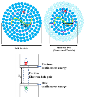
Graphene Quantum Dot-Based Organic Solar Cells

Quantum Dot Sensitized Solar Cells (QDSSCs)

Quantum Dots in Green Photocatalytic Applications for Degradation of Environmental Pollutants and Hydrogen Evolution
Clean Energy Reviews, Most Efficient Solar Panels. https://www.cleanenergyreviews.info/blog/most-efficient-solar-panels (2023)
P.V. Magazine, Longi claims 25.19% efficiency for p-type TOPCon solar cell. https://www.pv-magazine.com/2021/07/21/longi-claims-25-19-efficiency-for-p-type-topcon-solar-cell/
A.M. Cant, F. Huang, X.L. Zhang, Y. Chen, Y.B. Cheng, R. Amal, Tailoring the conduction band of titanium dioxide by doping tungsten for efficient electron injection in a sensitized photoanode. Nanoscale 6 , 3875 (2014)
Google Scholar
P.V. Kamat, Meeting the clean energy demand: Nanostructure architectures for solar energy conversion. J. Phys. Chem. 111 (7), 2834 (2007)
H. Tsubomura, M. Matsumura, Y. Nomura, T. Amamiya, Dye sensitized zinc oxide: aqueous electrolyte: platinum photocell. Nature 261 , 402 (1976)
H.K. Jun, M.A. Careem, A.K. Arof, Quantum dot sensitized solar cells-perspective and recent developments: a review of Cd chalcogenide quantum dots as sensitizers. Renew. Sustain. Energy Rev. 22 , 148 (2013)
A.P. Alivisators, Semiconductor clusters, nanocrystals and quantum dots. Science 271 , 933 (1996)
S. Pandey, D. Bodas, High quality quantum dots for multiplexed imaging: a critical review. Adv. Colloid Interface 278 , 102137 (2020)
A.I. Ekimov, A.A. Onushchenko, Quantum size effect in three dimensional microscopic semiconductor crystals. JETP Lett. 34 , 345 (1981)
S. Baskoutas, A.F. Terzis, Size-dependent band gap of colloidal quantum dots. J. Appl. Phys. 99 , 013708 (2006)
D. Segets, J.M. Lucas, R.N.K. Taylor, M. Scheele, H. Zheng, A.P. Alivisatos, W. Peukert, Determination of the quantum dot band gap dependence on particle size from optical absorbance and transmission electron microscopy measurements. ACS Nano 6 , 902132 (2012)
I. Moreels, K. Lambert, D. Smeets, D. De Muynck, T. Nollet, J.C. Martins, F. Vanhaecke, A. Vantomme, C. Delerue, G. Allan, Z. Hens, Size-dependent optical properties of colloidal PbS quantum dots. ACS Nano 3 , 302330 (2009)
A.D. Yoffe, Low-dimensional systems: quantum size effects and electronic properties of semiconductor microcrystallites (zero dimensional systems) and some quasi-two-dimensional systems. Adv. Phys. 42 (2), 173 (1993)
V.G. Plekhanov, Wannier-Mott excitons in isotope-disordered crystals. Rep. Prog. Phys. 61 , 1045 (1998)
L. Brus, Electronic wave functions in semiconductor clusters: experiment and theory. J. Phys. Chem. 90 (12), 2555 (1986)
T. Kippeny, L.A. Swafford, S.A. Rosenthal, Semiconductor nanocrystals: a powerful visual aid for introducing the particle in a box. J. Chem. Educ. 79 (9), 1094 (2002)
S. Lu, B. Wu, Y. Sun, Y. Cheng, F. Liao, M. Shao, Photoluminescence of pure silicon quantum dots embedded in an amorphous silica wire array. J. Mater. Chem. C 5 , 6713 (2017)
R.S. Yadav, P. Mishra, R. Mishra, M. Kumar, A.C. Pandey, Growth mechanism and optical property of CdS nanoparticles synthesized using amino-acid histidine as chelating agent under sonochemical process. Ultrason. Sonochem. 17 (1), 116 (2010)
K. Kyhm, J.H. Kim, S.M. Kim, H.S. Yang, Gain dynamics and excitonic transition in CdSe colloidal quantum dots. Opt. Mater. 30 (1), 158 (2007)
N. Wang, Y. Yang, G. Yang, Great blue-shift of luminescence of ZnO nanoparticle array constructed from ZnO quantum dots. Nanoscale Res Lett. 6 (1), 338 (2011)
I. Kang, F.W. Wise, Electronic structure and optical properties of PbS and PbSe quantum dots. J. Opt. Soc. Am. B 14 , 1632 (1997)
S. Busatto, M. de Ruiter, J.T.B.H. Jastrzebski, W. Albrecht, V. Pinchetti, S. Brovelli, S. Bals, M.-E. Moret, C. de Mello Donega, Luminescent colloidal InSb quantum dots from in situ generated single-source precursor. ACS Nano 14 (10), 13146 (2020)
N. Chouhan, C.L. Yeh, S.-F. Hu, R.-S. Liu, W.-S. Chang, K.-H. Chen, Photocatalytic CdSe QDs-decorated ZnO nanotubes: an effective photoelectrode for splitting water. Chem. Commun. 47 , 3493 (2011)
R. Trevisán, P. Ródenas, V. González-Pedro, C. Sima, R. Sánchez, E.M. Barea, I. Mora-Seró, F. Fabregat-Santiago, S. Giménez, Harnessing infrared photons for photoelectrochemical hydrogen generation. A PbS quantum dot based “Quasi-Artificial Leaf. J. Phys. Chem. Lett. 4 (1), 1416 (2013)
J. Hensel, G. Wang, Y. Li, J.Z. Zhang, Synergetic effect of CdSe quantum dot sensitization and nitrogen doping of TiO 2 nanostructures for photoelectrochemical solar hydrogen generation. Nano Lett. 10 , 478 (2010)
A. Kongkanand, K. Tvrdy, M. Kuno, P.V. Kamat, Quantum dot solar cells. Tuning photoreponse through size and shape control of CdSe–TiO 2 architecture. J. Am. Soc. 130 , 4007 (2008)
A. Zaban, O.I. Micic, B.A. Gregg, A.J. Nozik, Photosensitization of nanoporous TiO 2 electrodes with InP quantum dots. Langmuir 14 (12), 3153 (1998)
M. Seol, H. Kim, W. Kim, K. Yong, Highly efficient photoelectrochemical hydrogen generation using a ZnO nanowire array and a CdSe/CdS co-sensitizer. Electrochem. Commun. 12 , 1416 (2010)
G. Wang, X. Yang, F. Qian, J.Z. Zhang, Y. Li, Double-sided CdS and CdSe quantum dot Co-sensitized ZnO nanowire arrays for photoelectrochemical hydrogen generation. Nano Lett. 10 (3), 1088 (2010)
O.E. Semonin, J.M. Luther, S. Choi, H.-Y. Chen, J. Gao, A.J. Nozik et al., Peak external photocurrent quantum efficiency exceeding 100% via MEG in a quantum dot solar cell. Science 334 , 15303 (2011)
M.C. Hanna, R.J. Ellingson, M. Beard, P. Yu, O.I. Micic, A.J. Nozik, Quantum Dots Solar Cells: High Efficiency Through Multiple Exciton Generation . National Renewable Energy Lab (2004), pp. 25–28. https://www.osti.gov/servlets/purl/860690
V.I. Klimov, Spectral and dynamical properties of multiexcitons in semiconductor nanocrystals. Annu. Rev. Phys. Chem. 58 , 635 (2007)
M.C. Beard, R.J. Ellingson, Multiple exciton generation in semiconductor nanocrystals: toward efficient solar energy conversion. Laser Photonics Rev. 2 , 377 (2008)
A.J. Nozik, Multiple exciton generation in semiconductor quantum dots. Chem. Phys. Lett. 457 , 3 (2008)
A.J. Nozik, M.C. Beard, J.M. Luther, M. Law, R.J. Ellingson, J.C. Johnson, Semiconductor quantum dots and quantum dot arrays and applications of multiple exciton generation to third-generation photovoltaic solar cells. Chem. Rev. 110 , 6873 (2010)
A.J. Nozik, Nanoscience and nanostructures for photovoltaics and solar fuels. Nano Lett. 10 , 2735 (2010)
R.D. Schaller, M.A. Petruska, V.I. Klimov, Effect of electronic structure on carrier multiplication efficiency: comparative study of PbSe and CdSe nanocrystals. Appl. Phys. Lett. 87 , 253102 (2005)
R.D. Schaller, M. Sykora, S. Jeong, V.I. Klimov, High-efficiency carrier multiplication and ultrafast charge separation in semiconductor nanocrystals studied via time-resolved photoluminescence. J. Phys. Chem. B 110 , 25332 (2006)
J.E. Murphy, M.C. Beard, A.G. Norman, S.P. Ahrenkiel, J.C. Johnson, P. Yu, O.I. Mićić, R.J. Ellingson, A.J. Nozik, PbTe colloidal nanocrystals: synthesis, characterization, and multiple exciton generation. J. Am. Chem. Soc. 128 , 3241 (2006)
J.J.H. Pijpers, E. Hendry, M.T.W. Milder, R. Fanciulli, J. Savolainen, J.L. Herek, D. Vanmaekelbergh, S. Ruhman, D. Mocatta, D. Oron, A. Aharoni, U. Banin, M. Bonn, Carrier multiplication and its reduction by photodoping in colloidal InAs quantum dots. J. Phys. Chem. C 112 , 4783 (2008)
R.D. Schaller, J.M. Pietryga, V.I. Klimov, Carrier multiplication in InAs nanocrystal quantum dots with an onset defined by the energy conservation limit. Nano Lett. 7 , 3469 (2007)
S.K. Stubbs, S.J.O. Hardman, D.M. Graham, B.F. Spencer, W.R. Flavell, P. Glarvey, O. Masala, N.L. Pickett, D.J. Binks, Efficient carrier multiplication in InP nanoparticles. Phys. Rev. B 81 , 081303 (2010)
M.C. Beard, K.P. Knutsen, P. Yu, J.M. Luther, Q. Song, W.K. Metzger, R.J. Ellingson, A.J. Nozik, Multiple exciton generation in colloidal silicon nanocrystals. Nano Lett. 7 , 2506 (2007)
D. Gachet, A. Avidan, I. Pinkas, D. Oron, An upper bound to carrier multiplication efficiency in type II colloidal quantum dots. Nano Lett. 10 , 164 (2010)
H.M. Chen, C.K. Chen, Y.C. Chang, C.W. Tsai, R.S. Liu, S.F. Hu, W.S. Chang, K.H. Chen, Quantum dot monolayer sensitized ZnO nanowire-array photoelectrodes: true efficiency for water splitting. Angew. Chem. Int. Ed. 49 , 5966 (2010)
G. Nair, M.G. Bawendi, Carrier multiplication yields of CdSe and CdTe nanocrystals by transient photoluminescence spectroscopy. Phys. Rev. B Condens. Matter. Mater. Phys. 76 , 081304 (2007)
G. Nair, S.M. Geyer, L.Y. Chang, M.G. Bawendi, Carrier multiplication yields in PbS and PbSe nanocrystals measured by transient photoluminescence. Phys. Rev. B Condens. Matter Mater. Phys. 78 , 125325 (2008)
M. Ben-Lulu, D. Mocatta, M. Bonn, U. Banin, S. Ruhman, On the absence of detectable carrier multiplication in a transient absorption study of InAs/CdSe/ZnSe core/Shell1/Shell2 quantum dots. Nano Lett. 8 , 1207 (2008)
G. Yang, M. Kazes, D. Raanan, D. Oron, Bright near-infrared to visible upconversion double quantum dots based on a Type-II/Type-I heterostructure. ACS Photonics 8 (7), 1909 (2021)
N. Tripathi, M. Ando, T. Akai, K. Kamada, Efficient NIR-to-visible upconversion of surface-modified PbS quantum dots for photovoltaic devices. ACS Appl. Nano Mater. 4 (9), 9680 (2021)
K. Jiang, Y. Wang, X. Gao, C. Cai, H. Lin, Quick, and gram-scale synthesis of ultralong-lifetime room-temperature phosphorescent carbon dots by microwave irradiation. Angew. Chem. Int. Ed. 57 , 6216 (2018)
C. Hu, M. Li, J. Qiu, Y.P. Sun, Design and fabrication of carbon dots for energy conversion and storage. Chem. Soc. Rev. 48 , 2315 (2019)
M.L. Liu, B.B. Chen, C.M. Li, C.Z. Huang, Carbon dots: synthesis, formation mechanism, fluorescence origin and sensing applications. Green Chem. 21 , 449 (2019)
S. Zhu, Y. Song, X. Zhao, J. Shao, J. Zhang, B. Yang, The photoluminescence mechanism in carbon dots (graphene quantum dots, carbon nanodots, and polymer dots): current state and future perspective. Nano Res. 8 , 355 (2015)
V.C. Hoang, K. Dave, V.G. Gomes, Carbon quantum dot based composites for energy storage and electrocatalysis: mechanism applications and future prospects. Nano Energy 66 , 104093 (2019)
Z. Zhang, G. Yi, P. Li, X. Zhang, H. Fan, Y. Zhang, X. Wang, C. Zhang, A minireview on doped carbon dots for photocatalytic and electrocatalytic applications. Nanoscale 12 , 13899 (2020)
F. Yuan, Y.K. Wang, G. Sharma, Y. Dong, X. Zheng, P. Li, A. Johnston, G. Bappi, J.Z. Fan, H. Kung, B. Chen, M.I. Saidaminov, K. Singh, O. Voznyy, O.M. Bakr, Z.H. Lu, E.H. Sargent, Bright high-colour-purity deep-blue carbon dot light-emitting diodes via efficient edge amination. Nat. Photonics 14 , 171 (2020)
Y. Deng, M. Chen, G. Chen, W. Zou, Y. Zhao, H. Zhang, Q. Zhao, Visible-ultraviolet upconversion carbon quantum dots for enhancement of the photocatalytic activity of titanium dioxide. ACS Omega 6 (6), 4247 (2021)
Y. Yan, J. Gong, J. Chen, Z. Zeng, W. Huang, K. Pu, J. Liu, P. Chen, Recent advances on graphene quantum dots: from chemistry and physics to applications. Adv. Mater. 31 , 1808283 (2019)
A. Sahu, A. Garg, A. Dixit, A review on quantum dot sensitized solar cells: past, present and future towards carrier multiplication with a possibility for higher efficiency. Sol. Energy 203 , 210 (2020)
E.M. Barea, M. Shalom, S. Gimenez, I. Hod, I. Mora-Sero, A. Zaban, J. Bisquert, Design of injection and recombination in quantum dot sensitized solar cells. J. Am. Chem. Soc. 132 , 6834 (2010)
J. Chen, J. Wu, W. Lei, J.L. Song, W.Q. Deng, X.W. Sun, Co-sensitized quantum dot solar cell based on ZnO nanowire. Appl. Surf. Sci. 256 , 7438 (2010)
V. Gonzalez-Pedro, X. Xu, I. Mora-Sero, J. Bisquert, Modeling high-efficiency quantum dot sensitized solar cells. ACS Nano 4 , 5783 (2010)
Q. Zhang, X. Guo, X. Huang, S. Huang, D. Li, Y. Luo, Q. Shen, T. Toyoda, Q. Meng, Highly efficient CdS/CdSe-sensitized solar cells controlled by the structural properties of compact porous TiO 2 photoelectrodes. Phys. Chem. Chem. Phys. 13 (10), 4659 (2011)
X.-Y. Yu, B.-X. Lei, D.-B. Kuang, C.-Y. Su, Highly efficient CdTe/CdS quantum dot sensitized solar cells fabricated by a one-step linker assisted chemical bath deposition. Chem. Sci. 2 , 1396 (2011)
M.A. Hossain, J.R. Jennings, C. Shen, J.H. Pan, Z.Y. Koh, N. Mathews, Q. Wang, CdSe sensitized mesoscopic TiO 2 solar cells exhibiting >5% efficiency: redundancy of CdS buffer layer. J. Mater. Chem. 22 , 16235 (2012)
Y. Liu, Z. Wang, L. Li, S. Gao, D. Zheng, X. Yu, Q. Wu, Q. Yang, D. Zhu, W. Yang, Y. Xiong, Highly efficient quantum-dot-sensitized solar cells with composite semiconductor of ZnO nanorod and oxide inverse opal in photoanode. Electrochim. Acta 412 , 140145 (2022)
P.K. Santra, P.V. Kamat, Mn-doped quantum dot sensitized solar cells: a strategy to boost efficiency over 5%. J. Am. Chem. Soc. 134 , 2508 (2012)
J. Wang, Y. Li, Q. Shen, T. Izuishi, Z. Pan, K. Zhao, X. Zhong, Mn doped quantum dot sensitized solar cells with power conversion efficiency exceeding 9%. J. Mater. Chem. A 4 , 877 (2016)
R. Vogel, K. Pohl, H. Weller, Sensitization of highly porous, polycrystalline TiO 2 electrodes by quantum sized CdS. Chem. Phys. Lett. 174 , 241 (1990)
H. Song, Y. Lin, Z. Zhang, H. Rao, W. Wang, Y. Fan, Z. Pan, X. Zhong, Improving the efficiency of quantum dot sensitized solar cells beyond 15% via secondary deposition. J. Am. Chem. Soc. 143 (12), 4790 (2021)
A.J. Zavaraki, J. Huang, Y. Ji, H. Ågren, Low toxic Cu 2 GeS 3 /InP quantum dot sensitized infrared solar cells. J. Renew. Sustain. Energy 10 , 043710 (2018)
M. Ma, X. Hu, C. Zhang, C. Deng, X. Wang, The optimum parameters to synthesize bright and stable graphene quantum dots by hydrothermal method. J. Mater. Sci. Mater. Electron 28 , 6493 (2017)
S. Zhuo, M. Shao, S.T. Lee, Upconversion and downconversion fluorescent graphene quantum dots: ultrasonic preparation and photocatalysis. ACS Nano 6 (2), 1059 (2012)
D. Jiang, Y. Chen, N. Li, W. Li, Z. Wang, J. Zhu, H. Zhang, B. Liu, S. Xu, Synthesis of luminescent graphene quantum dots with high quantum yield and their toxicity study. PLoS ONE 10 , 1 (2015)
L. Liu, X. Yu, Z. Yi, F. Chi, H. Wang, Y. Yuan, D. Li, K. Xu, X.-W. Zhang, High efficiency solar cells tailored by biomass-converted graded carbon quantum dots. Nanoscale 10 , 1039 (2019)
K.A. Ritter, J.W. Lyding, The influence of edge structure on the electronic properties of graphene quantum dots and nanoribbons. Nat. Mater. 8 , 235 (2009)
C. Chung, Y.-K. Kim, D. Shin, S.-R. Ryoo, B.H. Hong, D.-H. Min, Biomedical applications of graphene and graphene oxide. Acc. Chem. Res. 46 , 2211 (2013)
T.-H. Han, Y. Lee, M.-R. Choi, S.-H. Woo, S.-H. Bae, B.H. Hong, J.-H. Ahn, T.-W. Lee, Extremely efficient flexible organic light-emitting diodes with modified graphene anode. Nat. Photon. 6 , 105 (2012)
J. Wu, M. Agrawal, H.A. Becerril, Z. Bao, Z. Liu, Y. Chen, P. Peumans, Organic light-emitting diodes on solution-processed graphene transparent electrodes. ACS Nano 4 , 43 (2010)
J.T.-W. Wang, J.M. Ball, E.M. Barea, A. Abate, J.A. Alexander-Webber, J. Huang, M. Saliba, I. Mora-Sero, J. Bisquert, H.J. Snaith, R.J. Nicholas, Low-temperature processed electron collection layers of graphene/TiO 2 nanocomposites in thin film perovskite solar cells. Nano Lett. 14 , 724 (2014)
N.G. Sahoo, Y. Pan, L. Li, S.H. Chan, Graphene-based materials for energy conversion. Adv. Mater 24 , 4203 (2012)
D.K. Kumar, D. Suazo-Davila, D. García-Torres, N.P. Cook, A. Ivaturi, M.-H. Hsu, A.A. Martí, C.R. Cabrera, B. Chen, N. Bennett, H.M. Upadhyaya, Low-temperature titania-graphene quantum dots paste for flexible dye-sensitised solar cell applications. Electrochim. Acta 305 , 278 (2019)
M. Dutta, S. Sarkar, T. Ghosh, D. Basak, ZnO/graphene quantum dot solid-state solar cell. J. Phys. Chem. C 116 (38), 20127 (2012)
Q. Zhao, R. Han, A.R. Marshall, S. Wang, B.M. Wieliczka, J. Ni, J. Zhang, J. Yuan, J.M. Luther, A. Hazarika, G.-R. Li, Colloidal quantum dot solar cells: progressive deposition techniques and future prospects on large-area fabrication. Adv. Mater. 34 , 2107888 (2022)
T. Kim, X. Jin, J.H. Song, S. Jeong, T. Park, Efficiency limit of colloidal quantum dot solar cells: effect of optical interference on active layer absorption. ACS Energy Lett. 5 (1), 248 (2020)
I. Mora-Sero, Current challenges in the development of quantum dot sensitized solar cells. Adv. Energy Mater 10 , 2001774 (2020)
M. Momirlan, T.N. Veziroglu, Current status of hydrogen energy. Renew. Sustain. Energy Rev. 6 (1–2), 141 (2002)
W.B. Ingler, S.U.M. Khan, Photoresponse of spray pyrolytically synthesized magnesium-doped iron(III) oxide (p-Fe 2 O 3 ) thin films under solar simulated light illumination. Thin Solid Films 461 , 301 (2004)
L. Li, H. Dai, L. Feng, D. Luo, S. Wang, X. Sun, Enhance photoelectrochemical hydrogen-generation activity and stability of TiO 2 nanorod arrays sensitized by PbS and CdS quantum dots under UV-visible light. Nanoscale Res. Lett. 10 , 418 (2015)
J. Liu, H. Zhang, F. Navarro-Pardo, G.S. Selopal, S. Sun, Z.M. Wang, H. Zhao, F. Rosei, Hybrid surface passivation of PbS/CdS quantum dots for efficient photoelectrochemical hydrogen generation. Appl. Surf. Sci. 530 , 47252 (2020)
P. Rodenas, T. Song, P. Sudhagar, G. Marzari, H. Han, L. Badia-Bou, S. Gimenez, F. Fabregat-Santiago, I. Mora-Sero, J. Bisquert, U. Paik, Y.S. Kang, Quantum dot based heterostructures for unassisted photoelectrochemical hydrogen generation. Adv. Energy Mater. 3 (2), 176 (2013)
Y.-X. Yu, W.-X. Ouyang, Z.-T. Liao, B.-B. Du, W.-D. Zhang, Construction of ZnO/ZnS/CdS/CuInS 2 core-shell nanowire arrays via ion exchange: p – n junction photoanode with enhanced photoelectrochemical activity under visible light. ACS Appl. Mater. Interfaces 6 (11), 8467 (2014)
W. Li, H. Geng, L. Yao, K. Cao, P. Sheng, Q. Cai, Photoelectrocatalytic hydrogen generation enabled by CdS passivated ZnCuInSe quantum dot-sensitized TiO 2 decorated with Ag nanoparticles. Nanomaterials 9 (3), 393 (2019)
J. Miao, H.B. Yang, S.Y. Khoo, B. Liu, Electrochemical fabrication of ZnO–CdSe core-shell nanorod arrays for efficient photoelectrochemical water splitting. Nanoscale 5 (22), 11118 (2013)
H. Zhang, L.V. Besteiro, J. Liu, C. Wang, G.S. Selopal, Z. Chen, D. Barba, Z.M. Wang, H. Zhao, G.P. Lopinski, S. Sun, F. Rosei, Efficient and stable photoelectrochemical hydrogen generation using optimized colloidal heterostructured quantum dots. Nano Energy 79 , 105416 (2021)
K. Kim, M.-J. Kim, S.-I. Kim, J.-H. Jang, Towards visible light hydrogen generation: quantum dot-sensitization via efficient light harvesting of hybrid-TiO 2 . Sci. Rep. 3 , 3330 (2013)
T. Bak, J. Nowotny, M. Rekas, C.C. Sorrell, Photo-electrochemical hydrogen generation from water using solar energy. Materials-related aspects. Int. J. Hydrog. Energy 27 , 991 (2022)
D. Wei, G. Amaratunga, Photoelectrochemical cell and its applications in optoelectronics. Int. J. Electrochem. Sci. 2 , 897 (2007)
X. Zhang, F. Wang, H. Huang, H. Li, X. Han, Y. Liu, Z. Kang, Carbon quantum dot sensitized TiO 2 nanotube arrays for photoelectrochemical hydrogen generation under visible light. Nanoscale 5 (6), 2274 (2013)
X. Zhang, H. Huang, J. Liu, Y. Liu, Z. Kang, Carbon quantum dots serving as spectral converters through broadband upconversion of near-infrared photons for photoelectrochemical hydrogen generation. J. Mater. Chem. A 1 , 11529 (2013)
X. Yu, R. Liu, G. Zhang, H. Cao, Carbon quantum dots as novel sensitizers for photoelectrochemical solar hydrogen generation and their size-dependent effect. Nanotechnology 24 (33), 335401 (2013)
H. Li, X. He, Z. Kang, Y. Liu, J. Liu, S. Lian, C.H.A. Tsang, X.B. Yang, S.-T. Lee, H. Huang, Water-soluble fluorescent carbon quantum dots and photocatalyst design. Angew. Chem. Int. Ed. 49 , 4430 (2010)
Y. Yao, G. Li, S. Ciston, R.M. Lueptow, K.A. Gray, Photoreactive TiO 2 /carbon nanotube composites: synthesis and reactivity. Environ. Sci. Technol. 42 , 4952 (2008)
H. Zhang, H. Ming, S. Lian, H. Huang, H. Li, L. Zhang, Y. Liu, Z. Kang, S.T. Lee, Fe 2 O 3 /carbon quantum dots complex photocatalysts and their enhanced photocatalytic activity under visible light. Dalton Trans. 40 , 10822 (2011)
H. Zhang, H. Huang, H. Ming, H. Li, L. Zhang, Y. Liu, Z. Kang, Carbon quantum dots/Ag 3 PO 4 complex photocatalysts with enhanced photocatalytic activity and stability under visible light. J. Mater. Chem. 22 , 10501 (2012)
H. Yu, H. Zhang, H. Huang, Y. Liu, H. Li, H. Ming, Z. Kang, ZnO/carbon quantum dots nanocomposites: one-step fabrication and superior photocatalytic ability for toxic gas degradation under visible light at room temperature. New J. Chem. 36 , 1031 (2012)
B.Y. Yu, S.-Y. Kwak, Carbon quantum dots embedded with mesoporous hematite nanospheres as efficient visible light-active photocatalysts. J. Mater. Chem. 22 , 8345 (2012)
C.X. Guo, Y. Dong, H.B. Yang, C.M. Li, Graphene quantum dots as a green sensitizer to functionalize ZnO nanowire arrays on F-doped SnO 2 Glass for enhanced photoelectrochemical water splitting. Adv. Energy Mater. 3 (8), 997 (2013)
Y. Yan, J. Chen, N. Li, J. Tian, K. Li, J. Jiang, J. Liu, Q. Tian, P. Chen, Systematic bandgap engineering of graphene quantum dots and applications for photocatalytic water splitting and CO 2 reduction. ACS Nano 12 (4), 3523 (2018)
Z. Zeng, F.-X. Xiao, X. Gui, R. Wang, B. Liu, T.T.Y. Tan, Layer-by-layer assembly of nitrogen-doped graphene quantum dots monolayer decorated one-dimensional semiconductor nanoarchitectures for solar-driven water splitting. J. Mater Chem. 4 , 16383 (2016)
Z. Xu, M. Yin, J. Sun, G. Ding, L. Lu, P. Chang, X. Chen, D. Li, 3D periodic multiscale TiO 2 architecture: a platform decorated with graphene quantum dots for enhanced photoelectrochemical water splitting. Nanotechnology 27 (11), 115401 (2016)
Y. Yan, D. Zhai, Y. Liu, J. Gong, J. Chen, P. Zan, Z. Zeng, S. Li, W. Huang, P. Chen, van der Waals heterojunction between a bottom-up grown doped graphene quantum dot and graphene for photoelectrochemical water splitting. ACS Nano 14 (1), 1185 (2020)
J.-W. Lee, D.-Y. Son, T.K. Ahn, H.-W. Shin, I.Y. Kim, S.-J. Hwang, M.J. Ko, S. Sul, H. Han, N.-G. Park, Quantum-dot-sensitized solar cell with unprecedentedly high photocurrent. J. Nat. 3 , 1050 (2013)
N. Guijarro, E. Guillén, T. Lana-Villarreal, R. Gómez, Quantum dot-sensitized solar cells based on directly adsorbed zinc copper indium sulfide colloids. Phys. Chem. Chem. Phys. 16 , 9115 (2014)
Y. Gao, X. Zou, Z. Huang, Doped heterojunction used in quantum dot sensitized solar cell. Int. J. Photoenergy 2014 , 179289 (2014)
Z. Huang, X. Zou, Superior photocurrent of quantum dot sensitized solar cells based on PbS: In/CdS quantum dots. Int. J. Photoenergy 2015 , 657871 (2015)
Y.-D. Hsieh, M.-W. Lee, G.-J. Wang, Sb 2 S 3 quantum-dot sensitized solar cells with silicon nanowire photoelectrode. Int. J. Photoenergy 2015 , 213858 (2015)
K. Lu, Y. Wang, J. Yuan, Z. Cui, G. Shi, S. Shi, L. Han, C. Si, Y. Zhang, X. Ling, Z. Liu, L. Chi, J. Fan, W. Ma, Efficient PbS quantum dots solar cells employing conventional structure. J. Mater. Chem. A. 5 , 23960 (2017)
G. Shen, Z. Du, Z. Pan, J. Du, X. Zhong, Solar paint from TiO 2 particles supported quantum dots for photoanodes in quantum dot-sensitized solar cells. ACS Omega 3 (1), 1102 (2018)
W. Wang, L. Zhao, Y. Wang, W. Xue, F. He, Y. Xie, Y. Li, A facile secondary deposition for improving quantum dot loading in fabricating quantum dot solar cells. J. Am. Chem. Soc. 141 (10), 4300 (2019)
H. Zhang, W. Fang, W. Wang, N. Qian, X. Ji, Highly efficient Zn−Cu−In−Se quantum dot-sensitized solar cells through surface capping with ascorbic acid. ACS Appl. Mater. Interfaces 11 , 6927 (2019)
B. Fu, C. Deng, L. Yang, Efficiency enhancement of solid-state CuInS2 quantum dot-sensitized solar cells by improving the charge recombination. Nanoscale Res. Lett. 14 , 198 (2019)
P. Xu, X. Chang, R. Liu, L. Wang, X. Li, X. Zhang, X. Yang, D. Wang, W. Lu, Boosting power conversion efficiency of quantum dot-sensitized solar cells by integrating concentrating photovoltaic concept with double photoanodes. Nanoscale Res. Lett. 15 , 188 (2020)
Y. Lin, H. Song, J. Zhang, H. Rao, Z. Pan, X. Zhong, Hole transport materials mediating hole transfer for high efficiency quantum dot sensitized solar cells. J. Mater. Chem. A 9 , 997 (2021)
H. Song, Y. Lin, M. Zhou, H. Rao, Z. Pan, X. Zhong, Zn–Cu–In–S–Se quinary “green” alloyed quantum-dot-sensitized solar cells with a certified efficiency of 14.4%. Angew. Chem. Int. Ed. 60 , 6137 (2020)
H. Wang, P. Sun, S. Cong, J. Wu, L. Gao, Y. Wang, X. Dai, Q. Yi, G. Zou, Nitrogen-doped carbon dots for “green” quantum dot solar cells. Nanoscale Res. Lett. 11 , 27 (2016)
D.H. Wang, J.K. Kim, S.J. Kim, B.H. Hee, J.H. Park, Efficient solution-processed small-molecule solar cells by insertion of graphene quantum dots. Nanoscale 6 (24), 15175 (2014)
D. Carolan, C. Rocks, D.B. Padmanaban, P. Maguire, V. Svrcek, D. Mariotti, Environmentally friendly nitrogen-doped carbon quantum dots for next generation solar cells. Sustain. Energy Fuels 1 , 1611 (2017)
X. Guo, H. Zhang, H. Sun, M. Tade, S. Wang, Green synthesis of carbon quantum dots for sensitized solar cells. Chem. Photo. Chem. 1 (4), 116 (2017)
Y.-Q. Liu, H. Huang, J.-S. Zhai, M.-J. Ma, J.-J. Fan, Graphene quantum dots/CdS/CdSe co-sensitized solar cells. J. Inorg. Mater. 32 (10), 1042 (2017)
S. Diao, X. Zhang, Z. Shao, K. Ding, J. Jie, X. Zhang, 12.35% efficient graphene quantum dots/silicon heterojunction solar cells using graphene transparent electrode. Nano Energy 31 , 359 (2017)
Y. Wang, L. Yan, G. Ji, C. Wang, H. Gu, Q. Luo, Q. Chen, L. Chen, Y. Yang, C.-Q. Ma, X. Liu, Synthesis of N, S-doped carbon quantum dots for use in organic solar cells as the ZnO modifier to eliminate the light soaking effect. ACS Appl. Mater. Interfaces 11 (2), 2243 (2019)
T. Majumder, S. Dhar, P. Chakraborty, K. Debnath, S.P. Mondal, S, N co-doped graphene quantum dots decorated C doped ZnO nanotaper photoanodes for solar cells application. Nano 14 (1), 1950012 (2019)
P. Huang, S. Xu, M. Zhang, W. Zhong, Z. Xiao, Y. Luo, Modulation doping of absorbent cotton derived carbon dots for quantum dot-sensitized solar cells. Phys. Chem. Chem. Phys. 21 (47), 26133 (2019)
T. Majumder, S.P. Mondal, Graphene quantum dots as a green photosensitizer with carbon-doped ZnO nanorods for quantum-dot-sensitized solar cell application. Bull. Mater. Sci. 42 , 65 (2019)
M.V. Prabhagar, M.P. Kumar, C. Takahashi, S. Kundu, T. Narayanan, N. Tharangattu, D.K. Pattanayak, Boron-doped graphene quantum dots: an efficient photoanode for dye sensitized solar cell. New J. Chem. 43 , 14313 (2019)
P. Huang, S. Xu, M. Zhang, W. Zhong, Z. Xiao, Y. Luo, Carbon quantum dots improving photovoltaic performance of CdS quantum dot-sensitized solar cells. Opt. Mater. 110 , 110535 (2020)
Q. Sun, C. Shen, D. Wang, T. Zhang, H. Ban, Y. Shen, Z. Zhang, X.-L. Zhang, G. Yang, M. Wang, Efficient and stable large-area perovskite solar cells with inorganic perovskite/carbon quantum dot-graded heterojunction. Research 2021 , 9845067 (2021)
X. Zhao, Y. Wu, Z. Xia, S. Chang, Y. Shang, A. Cao, A GQD-based composite film as photon down-converter in CNT/Si solar cells. Nano Res. 4 , 3893 (2021)
X. Wang, H. Zhu, Y. Xu, H. Wang, Y. Tao, S. Hark, X. Xiao, Q. Li, Aligned ZnO/CdTe core-shell nanocable arrays on indium tin oxide: synthesis and photoelectrochemicalproperties. ACS Nano 4 (6), 3302 (2010)
A. Ikram, S. Sahai, S. Rai, S. Dass, R. Shrivastav, V.R. Satsangi, Enhanced photoelectrochemical conversion performance of ZnO quantum dots sensitized α-Fe 2 O 3 thin films. Int. J. Hydrog. Energy 40 (16), 5583 (2015)
W.-X. Ouyang, Y.-X. Yu, W.-D. Zhang, High and stable photoelectrochemical activity of ZnO/ZnSe/CdSe/Cu(x)S core-shell nanowire arrays: nanoporous surface with Cu(x)S as a hole mediator. Phys. Chem. Chem. Phys. 17 (22), 14827 (2015)
A. Ikram, S. Sahai, S. Rai, S. Dass, R. Shrivastav, V.R. Satsangi, Improved charge transportation at PbS QDs/TiO 2 interface for efficient PEC hydrogen generation. Phys. Chem. Chem. Phys. 18 (23), 15815 (2016)
R. Adhikari, K. Basu, Y. Zhou, F. Vetrone, D. Ma, S. Sun, F. Vidal, H. Zhao, F. Rosei, Heterostructured quantum dot architectures for efficient and stable photoelectrochemical hydrogen production. J. Mater. Chem. A 6 , 6822 (2018)
A. Ikram, S. Dass, R. Shrivastav, V.R. Satsangi, Integrating PbS quantum dots with hematite for efficient photoelectrochemical hydrogen production. Phys. Status Solidi (a) 216 (7), 1800839 (2019)
K. Wang, X. Tong, Y. Zhou, H. Zhang, F. Navarro-Pardo, G.S. Selopal, G. Liu, J. Tang, Y. Wang, S. Sun, D. Ma, Z. Wang, F. Vidal, H. Zhao, X. Sun, F. Rosei, Efficient solar-driven hydrogen generation using colloidal heterostructured quantum dots. J. Mater. Chem. A 7 , 14079 (2019)
S. Sahai, A. Ikram, S. Rai, S. Dass, R. Shrivastav, V.R. Satsangi, CdSe quantum dots sensitized nanoporous hematite for photoelectrochemical generation of hydrogen. Int. J. Hydrog. Energy 39 (23), 11860 (2014)
A. Ikram, S. Sahai, S. Rai, S. Dass, R. Shrivastav, V.R. Satsangi, Synergistic effect of CdSe quantum dots on photoelectrochemical response of electrodeposited α-Fe 2 O 3 films. J. Power Sources 267 , 664 (2014)
F. Wang, Y. Liu, Z. Ma, H. Li, Z. Kang, M. Shen, Enhanced photoelectrochemical response in SrTiO 3 films decorated with carbon quantum dots. New J. Chem. 37 (2), 290 (2013)
F. Nan, Z. Kang, J. Wang, M. Shen, L. Fang, Carbon quantum dots coated BiVO 4 inverse opals for enhanced photoelectrochemical hydrogen generation. Appl. Phys. Lett. 106 (15), 153901 (2015)
K.-Y. Yoon, H.-J. Ahn, M.-J. Kwak, P. Thiyagarajan, J.-H. Jang, Graphene quantum dot-protected cadmium selenide quantum dot-sensitized photoanode for efficient photoelectrochemical cells with enhanced stability and performance. Adv. Opt. Mater. 3 (7), 907 (2015)
N.M. Vuong, J.L. Reynolds, E. Conte, Y.-I. Lee, H:ZnO nanorod-based photoanode sensitized by CdS and carbon quantum dots for photoelectrochemical water splitting. J. Phys. Chem. C 119 (43), 24323 (2015)
P. Sudhagar, I. Herraiz-Cardona, H. Park, T. Song, S.H. Noh, S. Gimenez, I.M. Sero, F. Fabregat-Santiago, J. Bisquert, C. Terashima, U. Paik, Y.S. Kang, A. Fujishima, T.H. Han, Exploring graphene quantum dots/TiO 2 interface in photoelectrochemical reactions: solar to fuel conversion. Electrochim. Acta 187 , 249 (2016)
Z. Zhao, T. Butburee, P. Peerakiatkhajohn, M. Lyu, S. Wang, L. Wang, H. Zheng, Carbon quantum dots sensitized vertical WO3Nanoplates with enhanced photoelectrochemical properties. Chem. Sel. 1 (11), 2772 (2016)
K.-H. Ye, Z. Wang, J. Gu, S. Xiao, Y. Yuan, Y. Zhu, Y. Zhang, W. Mai, S. Yang, Carbon quantum dots as a visible light sensitizer to significantly increase the solar water splitting performance of bismuth vanadate photoanodes. Energy Environ. Sci. 10 (3), 772 (2017)
T. Majumder, S. Dhar, P. Chakraborty, K. Debnath, S.P. Mondal, Advantages of ZnO nanotaperphotoanodes in photoelectrochemical cells and graphene quantum dot sensitized solar cell applications. J. Electroanal. Chem. 813 , 92 (2018)
X. Wang, M. Wang, G. Liu, Y. Zhang, G. Han, A. Vomiero, H. Zhao, Colloidal carbon quantum dots as light absorber for efficient and stable ecofriendly photoelectrochemical hydrogen generation. Nano Energy 86 , 106122 (2021)
Download references
The authors declare that no funds, grants or other support were received during the preparation of this manuscript.
Author information
Authors and affiliations.
Department of Physics, St. John’s College, Agra, India
Sonal Sahai, Ashu Jangra & Lisy M. Thomas
Department of Physics and Computer Science, Dayalbagh Educational Institute, Agra, India
Vibha R. Satsangi
You can also search for this author in PubMed Google Scholar
Contributions
All authors contributed to the study conception and design. Sonal Sahai and Ashu Jangra collected the material and reviewed the literature for the purpose. Sonal Sahai, Lisy M Thomas and Vibha R Satsangi systemized, wrote and improved the draft of the paper. All authors read and approved the final manuscript.
Corresponding author
Correspondence to Sonal Sahai .
Ethics declarations
Conflict of interest.
The authors have no relevant financial or non-financial interests to disclose.
Additional information
Publisher's note.
Springer Nature remains neutral with regard to jurisdictional claims in published maps and institutional affiliations.
Rights and permissions
Springer Nature or its licensor (e.g. a society or other partner) holds exclusive rights to this article under a publishing agreement with the author(s) or other rightsholder(s); author self-archiving of the accepted manuscript version of this article is solely governed by the terms of such publishing agreement and applicable law.
Reprints and permissions
About this article
Sahai, S., Jangra, A., Thomas, L.M. et al. Quantum Dots as Efficient Solar Energy Absorber: Review on Photovoltaics and Photoelectrochemical Systems. J. Inst. Eng. India Ser. D 105 , 553–566 (2024). https://doi.org/10.1007/s40033-023-00490-x
Download citation
Received : 27 February 2023
Accepted : 03 May 2023
Published : 16 May 2023
Issue Date : April 2024
DOI : https://doi.org/10.1007/s40033-023-00490-x
Share this article
Anyone you share the following link with will be able to read this content:
Sorry, a shareable link is not currently available for this article.
Provided by the Springer Nature SharedIt content-sharing initiative
- Quantum dots
- Solar energy
- Photovoltaics
- Photoelectrochemical
- Find a journal
- Publish with us
- Track your research
IMAGES
VIDEO
COMMENTS
SUBJECTS: Diodes, Materials, Quantum dots, Thin films, Two dimensional materials. It has been many years since the first works on the reduced dimensionality of semiconductors, which led to the concept of "artificial atoms", or quantum dots (QDs). (1,2) These semiconductor nanocrystals, with nanometer-sized diameters, exhibit quantum size ...
QDs are tiny semiconductor nanoparticles [1, 2] just a few nanometers in size (ranging from a few nanometers to tens of nanometers) which possess one of the most important properties of quantum confinement [].Onyia et al [] theoretically studied the effect of quantum confinement on QDs using particles in a box model.More generally, when a system has one or more dimensions small enough to ...
Quantum dots are crystals of a fluorescent semiconductor material with a diameter of as few as 10 to 100 atoms (2-10 nm). They are used as labels for imaging molecules because of their very narrow ...
Highlights. •. Quantum Dots are fluorescence type semiconductor nano sized particles. •. Toxicity of quantum dots is depends upon the size, material used, dose, route of administration and capping material. •. The first clinical trial of quantum-dot technology in humans was approved by USFDA in 2011. •.
The confinement found in colloidal semiconductor quantum dots enables the design of materials with tunable properties. García de Arquer et al. review the recent advances in methods for synthesis and surface functionalization of quantum dots that enable fine tuning of their optical, chemical, and electrical properties.These important developments have driven the commercialization of display ...
The 2023 Nobel Prize in Chemistry was awarded to Alexei Ekimov, Louis Brus, and Moungi Bawendi for the discovery and development of quantum dots, an area of research ripe with exciting results in terms of both fundamental science and present and forthcoming applications. Quantum dots, with their colors and their intriguing properties, have fascinated and engaged generations of scientists over ...
Quantum dots (QDs) have sparked great interest due to their unique electronic, optical, and structural properties. In this review, we provide a critical analysis of the latest advances in the ...
Semiconductor quantum dots (QDs) are a customized synthetic equivalent to atoms that have found uses in a wide range of modern semiconductor devices 1.Nanostructures based solely on III-V-system ...
2.2.1 Surface Structure of Quantum Dots. The electronic states related to the surface have substantial out-come on the optical properties of dots. For instance, 5 nm cadmium sulfide (CdS) QDs have 15% atoms at their surface [].This is because of their unique property i.e. extraordinary surface to volume ratio, which permits boosted/hindered photo-generated charge carrier transfer rate from ...
It was work in progress, Brus reported 1. Just over 30 years later, that work has come to fruition with the award of the 2023 Nobel Prize in Chemistry to Brus and two other pioneers of quantum-dot ...
Generally, QDs have interesting features including small particle size, tunable composition and properties, high quantum yield, high brightness, and intermittent light emission (blinking), which have recruited them in versatile applications such as solar cells, LED technology, and biomedical applications including imaging, drug delivery, and cancer photodynamic therapy. 14-16 The tunable ...
1. Introduction. From solar panels to medical applications, quantum dots are receiving discernible attention in today's world due to their unparalleled and cutting-edge scope [1, 2].Quantum dots are colloidal semiconductor nanoparticles that exhibit a distinctive set of optical and transport properties due to their spatial confinement regime, also known as the quantum confinement effect.
Introduction. Quantum dots (QDs), also known as nanoscale semiconductor crystals, were first described by Ekimov and Onushenko 1 in a glass matrix, back in 1981, with the first biological imaging application reported in 1998. 2 Since then the field of QDs has been growing steadily and now includes applications in fields of solar cells, photovoltaic devices, light-emitting diode (LED ...
As new-generation solar cells, quantum dot-sensitized solar cells (QDSCs) have the outstanding advantages of low cost and high theoretical efficiency; thus, such cells receive extensive research attention. Their power conversion efficiency (PCE) has increased from 5% to over 15% in the past decade. However, compared with the theoretical efficiency (44%), the PCE of QDSCs still needs further ...
Semiconductor quantum dots have been a matter of significant research interest owing to their potential biomedical applications, especially in drug delivery, biosensing, and, bioimaging. Practical biomedical applications of quantum dots require high fluorescence quantum yield, good aqueous solubility, narrow size distribution, and crystallinity ...
Quantum dot semiconductors have gain great attraction for the development of high efficiency solar cells due to remarkable optoelectronic properties such as tunable bandgap, multiple exciton generation (MEG) and high extinction coefficient. Despite quantum dot solar cells having theoretical power conversion efficiency of about 66%, actual maximum efficiency is only 16.6%. So, it is important ...
Quantum dots (QDs) are semiconductor crystals in the nanodimension having unique optical and electronic properties that differ from bulk material due to quantum mechanics. The QDs have a narrow emission peak, size-dependent emission wavelength, and broad excitation range which can be utilized for diverse biomedical applications such as ...
Therefore the quantum efficiency in SCDQD structure enhances which leads to increasing the responsivity of the proposed system. The double barrier reduces the dark current. These improvements ...
But QDs lag far behind thin films in power conversion efficiency, with a previous certified cell record of 13.4% for QDs 1 compared to 25.2% for thin films 2. Writing in Nature Energy, Mengmeng ...
Quantum dots are so tiny that the electrons within them exist only in states with specific energies. As such, quantum dots behave similarly to atoms, and, like atoms, can achieve higher levels of energy when light stimulates them. Chakraborty works in theoretical and computational chemistry, meaning "we work with computers and computers only ...
Research efforts are being devoted to realize colloidal, heavy metal ion free, and luminescent quantum dots. We address radiative recombination in Zn alloyed CuGaS 2 /ZnS core/shell chalcopyrite quantum dots (CQDs) emitting in the blue-green spectral region. QDs show a systematic increase in the optical band gap and emission energy with an increasing amount of Zn in their core.
Abstract. Recent years have witnessed a giant leap in the synthesis and studies of Quantum dots (QDs). With their remarkable photophysical properties, QDs have emerged as an essential material in material science research. QDs are multifaceted, with their applications ranging from optical to next-generation theranostics.
Quantum dots are tiny particles or nanocrystals of a semiconducting material with diameters in the range of 2-10 nanometers (10-50 atoms). They were first discovered in 1980. 1 They display unique electronic properties, intermediate between those of bulk semiconductors and discrete molecules, that are partly the result of the unusually high surface-to-volume ratios for these particles. 2-4 The ...
2.1.1. Size versus Density of States . A most unique property of the Qdots is quantum confinement, which modifies the DOS near the band-edges. Schematic diagrams of the DOS as a function of energy in Figure 2 show that Qdots lie between the discrete atomic and continuous bulk materials. Quantum confinement effects are observed when the size is sufficiently small that the energy level spacing ...
A team of South Korean scientists led by Professor KIM Dae-Hyeong of the Center for Nanoparticle Research within the Institute for Basic Science has pioneered a novel approach to stretchable displays. The team announced the first development of intrinsically stretchable quantum dot light-emitting diodes (QLEDs).
The present study demonstrates the development of a thin film chemical sensor based on 2,4 Dinitro-1-chlorobenzene (DNCB) and carbon quantum dots (made from Phthalic acid and Tri-ethylene diamine (TED)) co-immobilized in chitosan based thin films for the specific detection of hydrazine.
Quantum dots (QDs) have enticed the researchers, due to their unconventional optical and electronic characteristics, contributing potentially for several applications such as biomedical, sensors, and optical and electronic devices. Properties like tunable band gap, multiple exciton generation and photoluminescence make them better suited for energy devices, pertaining to efficient energy ...
Program. Proposals submitted in response to DAF topics shall not include TABA. AIR FORCE PROPOSAL EVALUATIONS . Proposals will be evaluated for overall merit in accordance with the criteria discussed in the 24.2 BAA. DAF is seeking varying technical/scientific approaches and/or varying and new technologies